Low temperature drift voltage reference circuit

a voltage reference circuit and low temperature drift technology, applied in the field of electronic circuits, can solve the problems of difficult to adjust to obtain a different reference voltage, etc., and achieve the effect of expanding the scope of application and increasing process complexity and cos

Active Publication Date: 2015-11-24
BCD SHANGHAI MICRO ELECTRONICS CO LTD
View PDF5 Cites 0 Cited by
  • Summary
  • Abstract
  • Description
  • Claims
  • Application Information

AI Technical Summary

Benefits of technology

[0005]The inventors have observed that conventional E / D voltage reference circuits have many drawbacks. For example, the reference voltage provided by the circuit of FIG. 1 usually falls in a very narrow range centered around, e.g., 0.85 V, and it is difficult to make adjustment to obtain a different reference voltage. In addition, forming depletion-mode NMOS transistors would need to add an extra masking step to a standard integrated circuit manufacturing process, thus increasing process complexity and cost. In contrast, in embodiments of the present invention, the voltage reference circuits use depletion-mode PMOS transistors, which can be fabricated using standard CMOS process technology, and the threshold implant step for the depletion mode PMOS transistors can share the same mask and be carried out at the same time as the implant step for high value resistors. No extra masking step is needed. In embodiments of the invention, the voltage reference circuit is configured to operate in a large supply voltage range, which enables a large range of adjustable reference voltages. For example, a bias circuit is provided to maintain a depletion-mode PMOS transistor in the saturation region with a large Vds even under a low voltage supply. A feedback circuit is provided to maintain an enhancement-mode PMOS transistor in the saturation region even under a low voltage supply. For example, the voltage reference circuit according to some embodiments of the invention can operate with a supply voltage source of between 2V to 5V, greatly expanding its scope of application. In addition, the reference voltage can be adjusted in a wide range by varying the ratio of two high-value resistors.
[0006]According to an embodiment of the present invention, a voltage reference circuit includes a first enhancement-mode PMOS transistor, a first enhancement mode NMOS transistor, and a first depletion-mode PMOS transistor coupled in series between a voltage supply and a ground. The voltage reference circuit also includes a first resistive device, a feedback device, and a second resistive device coupled in series between the voltage supply and the ground. The feedback device is coupled to the first enhancement PMOS transistor to form a feedback circuit. A bias circuit is coupled to a gate of the first enhancement-mode NMOS transistor. The first enhancement-mode PMOS transistor and the first depletion-mode PMOS transistor are configured to operate in saturation region. A first reference voltage across the first resistive device and a second reference voltage across the second resistive device are configured to be independent of voltage supply variations and can have low temperature drift.

Problems solved by technology

For example, the reference voltage provided by the circuit of FIG. 1 usually falls in a very narrow range centered around, e.g., 0.85 V, and it is difficult to make adjustment to obtain a different reference voltage.
In addition, forming depletion-mode NMOS transistors would need to add an extra masking step to a standard integrated circuit manufacturing process, thus increasing process complexity and cost.

Method used


Image

  • Low temperature drift voltage reference circuit
  • Low temperature drift voltage reference circuit
  • Low temperature drift voltage reference circuit

Examples


Embodiment Construction

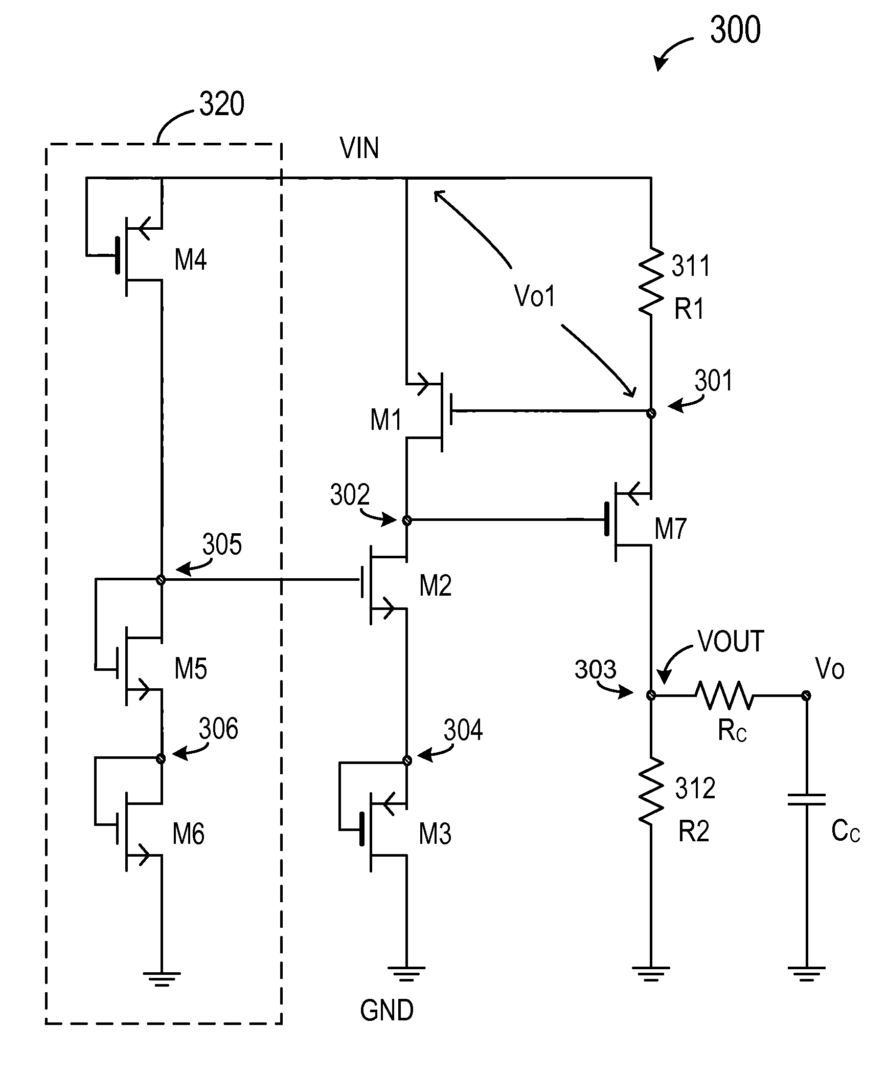
[0022]FIG. 2 is a schematic circuit diagram illustrating a voltage reference circuit 200 according to an embodiment of the present invention. As shown in FIG. 2, voltage reference circuit 200 includes a first enhancement-mode PMOS transistor M1, a first enhancement mode NMOS transistor M2, and a first depletion-mode PMOS transistor M3 coupled in series between a voltage supply VIN and a ground GND. The first depletion-mode PMOS transistor M3 has shorted gate and source. Voltage reference circuit 200 also includes a feedback device 230 coupled to a gate of the first enhancement PMOS transistor M1 at a first node 201. The feedback device is also coupled to a drain of the first enhancement-mode PMOS transistor M1 at a second node 202, forming a feedback circuit. A first resistive device 211 is coupled between the voltage supply VIN and the first node 201. A second resistive device 212 has one end coupled to the feedback device 230 at a third node 203, and has the other end coupled to t...


PUM


Abstract

A voltage reference circuit includes a first enhancement-mode PMOS transistor, a first enhancement mode NMOS transistor, and a first depletion-mode PMOS transistor coupled in series between a voltage supply and a ground. A second depletion-mode PMOS transistor is coupled to the first enhancement PMOS transistor to form a feedback circuit. A first resistive device is coupled between the voltage supply and the second depletion-mode PMOS transistor, and a second resistive device is coupled between the second depletion-mode PMOS transistor and the ground. A bias circuit is coupled to a gate of the first enhancement-mode NMOS transistor. The first enhancement-mode PMOS transistor and the first depletion-mode PMOS transistor are configured to operate in saturation region. A first reference voltage across the first resistor and a second reference voltage across the second resistor are configured to be independent of the magnitude of the voltage supply and have low temperature drift.

Description

CROSS-REFERENCES TO RELATED APPLICATIONS[0001]This application claims priority to Chinese Patent Application No: 201210385231.X, filed Oct. 11, 2012, commonly owned and incorporated by reference herein for all purposes.BACKGROUND OF THE INVENTION[0002]The present invention relates to the technical field of electronic circuits. More particularly, embodiments of the present invention relate to adjustable voltage reference circuits having low temperature drift.[0003]In electronic circuits, a voltage reference is an electronic device that ideally produces a fixed voltage irrespective of operating conditions, such as power supply variations and temperature changes. Voltage references are used in power management integrated circuit chips, analog-to-digital converters and digital-to-analog converters, and other measurement and control systems. The voltage reference often can determine the performance of power management integrated circuit chips. A reference voltage source can be implemente...

Claims


Application Information

Patent Timeline
Patent Type & Authority Patents(United States)
IPC IPC(8): H03K17/14G11C5/14G11C7/04
CPCG11C5/147G11C7/04
Inventor PENG, SHAOHUALIU, ZUTAO
Owner BCD SHANGHAI MICRO ELECTRONICS CO LTD
Why Eureka
Try Eureka