

Semiconductor optical device
a technology of semiconductor devices and optical devices, which is applied in semiconductor devices, solid-state devices, lighting and heating apparatus, etc., can solve the problems of reducing the area available on the top surface of the stem for mounting components, the inability of the resin cap to be secured to the stem by welding, and the inability to secure the resin cap to the stem, etc., to achieve accurate alignment and secure, the effect of maximizing the interior space of the cap
- Summary
- Abstract
- Description
- Claims
- Application Information
AI Technical Summary
Benefits of technology
Problems solved by technology
Method used
Image

Examples
first embodiment
Configuration of Device of First Embodiment
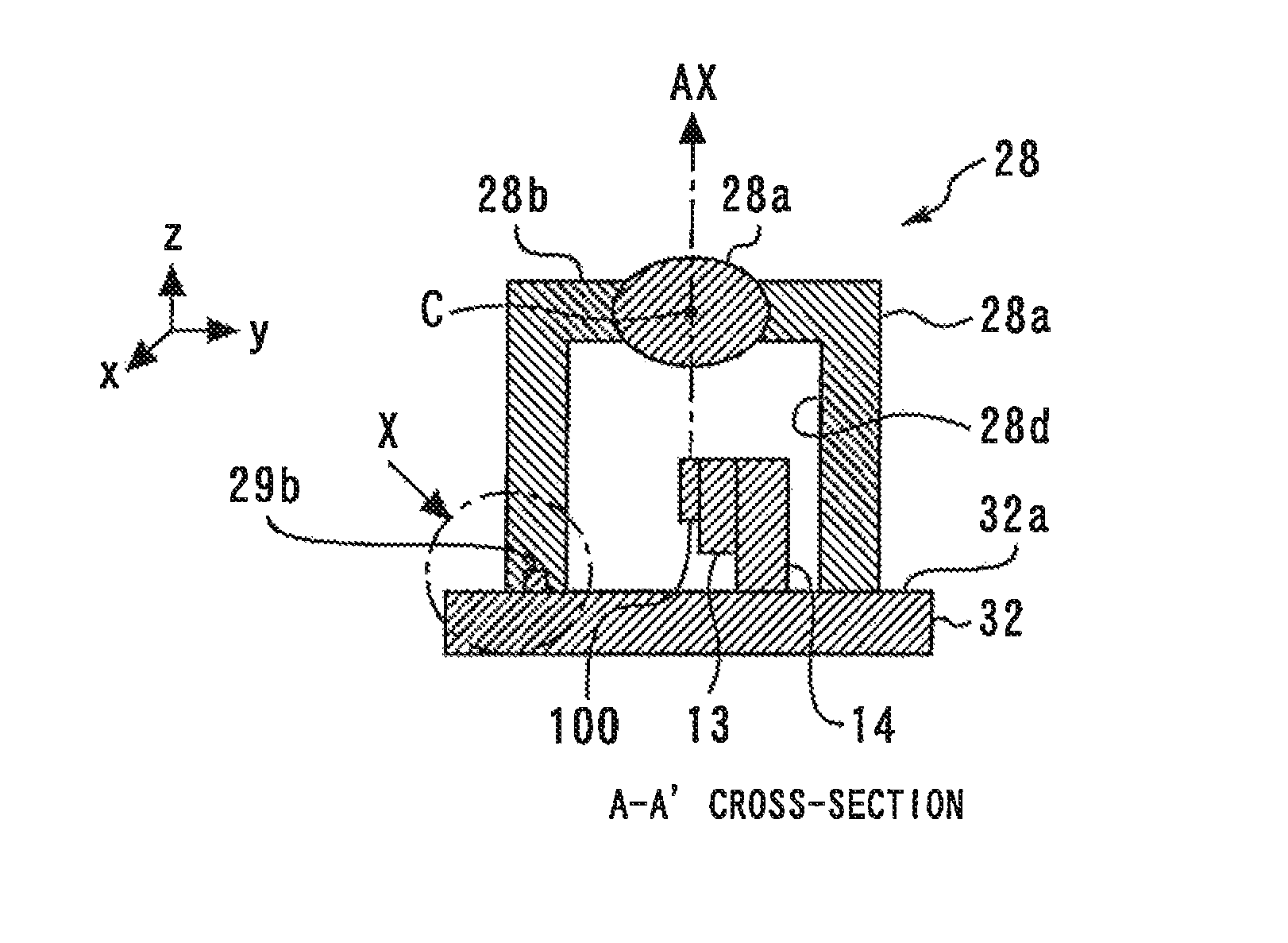
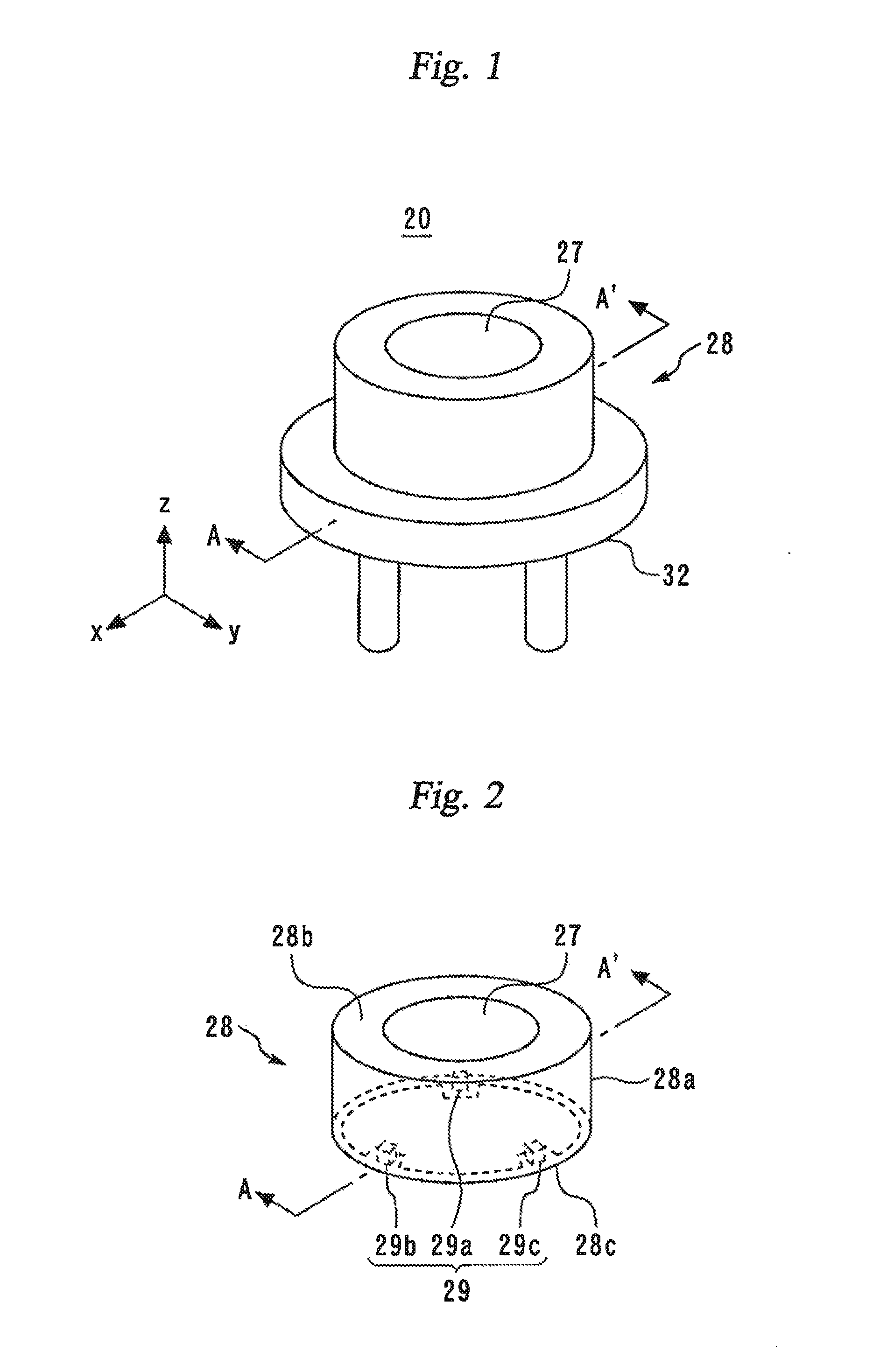
[0036]FIG. 1 is a perspective view of a semiconductor optical device 20 in accordance with a first embodiment of the present invention. In this embodiment, the semiconductor optical device 20 has a CAN package structure. Referring to FIG. 1, the semiconductor optical device 20 includes a stem 32 and a cap (or lid) 28 which is mounted on and covers the stem 32. The stem 32 and the cap 28 are bonded together by an adhesive. The space enclosed by the cap 28 and the stem 32 is sealed, and filled with a filler gas such as air, dry gas, or nitrogen gas.
(Configuration of Cap)
[0037]FIG. 2 is a perspective view of the cap 28 of the semiconductor optical device 20 of the first embodiment. The cap 28 is made of a resin. The cap 28 has a cylindrical body portion 28a. The cylindrical body portion 28a has an outside surface and an inside surface 28d which extend along the entire length of the cylindrical body portion 28a. The cap 28 has a plate portion 2...
second embodiment
[0077]FIG. 17 is a diagram illustrating a configuration of a semiconductor optical device in accordance with a second embodiment of the present invention. The semiconductor optical device of the second embodiment is similar to the semiconductor optical device 20 of the first embodiment, except that the second portions P2 of the cap have a different configuration.
[0078]FIG. 17 shows an enlarged cross-sectional view of a portion of the cap 728 of the semiconductor optical device of the second embodiment, which portion corresponds to the portion shown in dashed line X of FIG. 6. That is, the cross-section shown in FIG. 17 corresponds to the cross-sections shown in FIGS. 7 and 9A to 11B, and also corresponds to the cross-section shown in FIG. 14. The cap 728 is similar to the cap 328 described above with reference to FIGS. 10A and 10B, and the three second portions P2 of the cap 728 have the step portions 329a, 329b, and 329c, respectively. However, the cap 728 differs from the cap 328 ...
third embodiment
[0083]FIG. 21 is a diagram showing a configuration of a semiconductor optical device in accordance with a third embodiment of the present invention. Specifically, FIG. 21 shows the configuration of the cap 828 of the semiconductor optical device of the third embodiment. The cap 828 is similar in basic configuration to the cap 328 described above with reference to FIGS. 10A and 10B, and the three second portions P2 of the cap 828 have a step portion 329. However, the cap 828 differs from the cap 328 in that each step portion 329 (which constitutes a portion of the edge portion 328c of the cap 828) has a slit structure 800 formed in its surface. Except for this feature, the semiconductor optical device of the third embodiment is similar in configuration to the semiconductor optical device of the first embodiment.
[0084]Each slit structure 800 includes a plurality of parallel slits. Thus, in the third embodiment, the bottom surface of the edge portion 328c of the cap 828, which surface ...
PUM
 Abstract
Description
Claims
Application Information