
Common mode choke coil

a choke coil and common mode technology, applied in the direction of transformer/inductance coil/winding/connection, transformer/inductance magnetic core, inductance, etc., can solve the problem of increasing the insertion loss of a normal mode signal, the coupling degree between the primary coil and the secondary coil is difficult to make high, and the asymmetry of the signal lines is generated. problem, to achieve the effect of high coupling degree and high coupling degr

Active Publication Date: 2016-04-12
MURATA MFG CO LTD
View PDF20 Cites 2 Cited by
  • Summary
  • Abstract
  • Description
  • Claims
  • Application Information

AI Technical Summary

Benefits of technology

[0010]Preferred embodiments of the present invention provide a small-sized common mode choke coil having a small loss of a normal mode signal and a high ability to remove common mode noise.
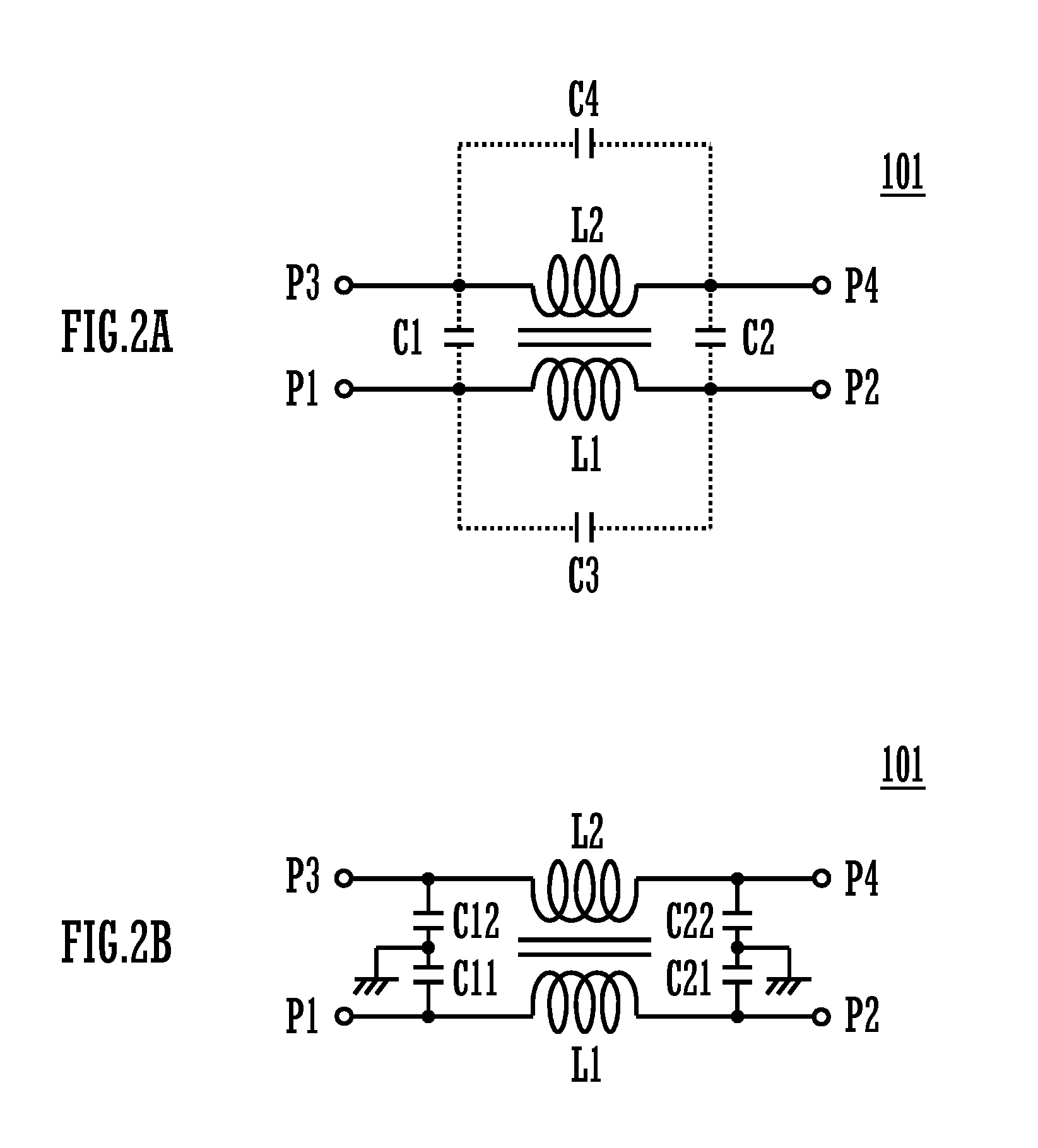
[0012]According to various preferred embodiments of the present invention, it is possible to achieve magnetic field coupling between the primary coil and the secondary coil with a high coupling degree without increasing capacitive coupling between the primary coil and the secondary coil. Hence, it is possible to obtain a small-sized common mode choke coil in which differential impedance is not apt to decrease regardless of a small insertion loss of a normal mode signal.

Problems solved by technology

However, in reality, especially on signal lines for the high-speed interface, a common mode noise current ascribed to the asymmetry of the signal lines is generated.
However, a coupling degree between the primary coil and the secondary coil is difficult to make high just by simply arraying the primary coil and the secondary coil in the laminating direction inside the laminated element body.
When the coupling degree between the primary coil and the secondary coil is low, an insertion loss of a normal mode signal increases.
When this capacitance increases, differential impedance of the common mode choke coil decreases, and becomes unable to be matched with impedance of the balanced transmission line.
Further, in the structure where the primary coil and the secondary coil are arrayed in the laminating direction inside the laminated element body, there occurs displacement of a formed position of a coil pattern or displacement of lamination of sheets due to a process problem.
Moreover, when the coils are mounted on a printed wiring board, a capacitance between the primary coil and a ground conductor and a capacitance between the secondary coil and the ground conductor becomes unbalanced due to a structural problem such as a difference in coupling amount between each coil and the ground conductor.
For this reason, the symmetry between the primary coil and the secondary coil cannot be ensured, leading to conversion of the common mode noise to the normal mode signal (noise).
Further, although a magnetic body may be used as the laminated element body, since the magnetic body has relatively large frequency dependence, a loss of the normal mode signal especially in a high frequency band is apt to become large.
Moreover, a sufficient coupling value between the primary coil and the secondary coil cannot be obtained especially in the high frequency band, and the loss of the normal mode signal is apt to become large.

Method used


Image

  • Common mode choke coil
  • Common mode choke coil
  • Common mode choke coil

Examples


first preferred embodiment

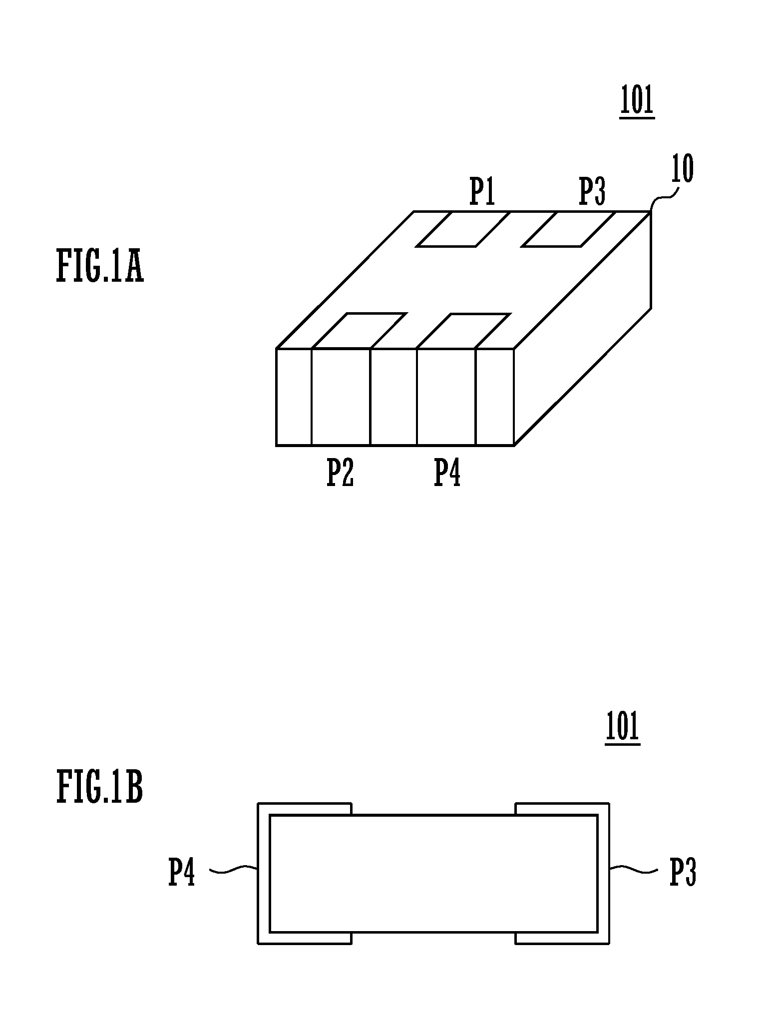
[0034]FIG. 1A is an external perspective view of a common mode choke coil 101 of a first preferred embodiment of the present invention, and FIG. 1B is a side view thereof.

[0035]As shown in FIGS. 1A and 1B, input / output terminals P1, P2, P3, P4 are provided on an external surface of a laminated element body 10.

[0036]In the case of a common mode choke coil for an HF (High Frequency) band, an eddy current loss is relatively small, and hence a magnetic material (dielectric material with a high magnetic permeability) can be used as a material for a base material layer in terms of containment properties of magnetic energy. As this magnetic material, a ferrite magnetic body adaptable to a high frequency, such as hexagonal ferrite, may be used. On the other hand, for example, in the case of forming a common mode choke coil for a UHF (Ultra High Frequency) band, it is preferable to use a dielectric material with high electric insulation resistance so as to suppress an eddy current loss in a ...

second preferred embodiment

[0069]In the second preferred embodiment of the present invention, a common mode choke coil including an ESD protective element is shown. FIG. 10 is an external perspective view of a common mode choke coil 102 of the second preferred embodiment. FIG. 11A is a sectional view of the common mode choke coil 102, and FIG. 11B is a sectional view of an ESD (Electrostatic Discharge) protective element section.

[0070]In this common mode choke coil 102, a similar conductor pattern to that of the common mode choke coil shown in the first preferred embodiment is provided in a lamination section LL2 in FIG. 11A. Then, ESD protective elements Dg1, Dg3 are provided in a lamination section LL1.

[0071]FIG. 11B is a sectional view of the ESD protective element Dg1 portion. In this example, a shield layer Sh11, a discharge auxiliary electrode Se1, discharge electrodes De11, De12, a hollow portion Ah1 and a shield layer Sh21 are provided.

[0072]FIG. 12 is a schematic diagram representing a cross-sectiona...

third preferred embodiment

[0096]FIG. 14 is a plan view of a common mode choke coil 103 according to a third preferred embodiment of the present invention. The input / output terminals p1, p2, p3, p4 are provided on the surface of the common mode choke coil 103.

[0097]FIG. 15 is an exploded plan view showing a conductor pattern and the like of each base material layer in the common mode choke coil of the third preferred embodiment. (1) is a plan view of a first layer (bottom layer), (2) is a plan view of a second layer, (3) is a plan view of a third layer, and (4) is a plan view of a top layer.

[0098]FIG. 16 is a view showing the connection relation of each conductor as to a pair of two layers which are adjacent in the layer direction out of the above four layers.

[0099]FIG. 17 is a sectional view along a line A-A in FIGS. 14 and 15. As represented in FIG. 17, the common mode choke coil 103 is provided with a substrate 20, and a plurality of linear conductors laminated on this substrate 20 via an interlayer insula...


PUM

PropertyMeasurementUnit
thicknessesaaaaaaaaaa
relative permittivity ∈raaaaaaaaaa

Abstract

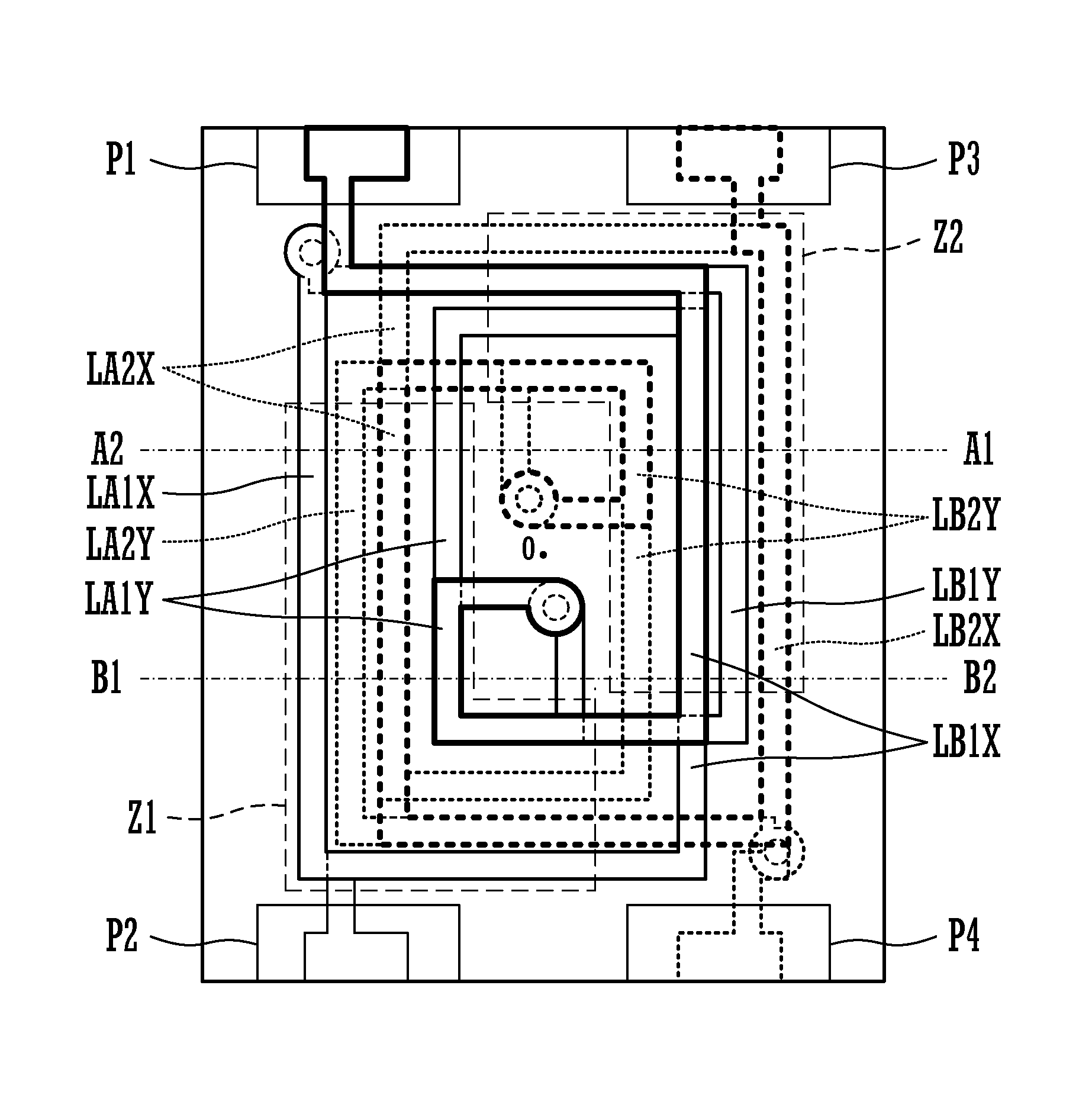
In a common mode choke coil, electrodes of input / output terminals are located on a bottom surface of a bottom layer. First linear conductors and second linear conductors are located on base material layers. A primary coil includes the first linear conductors and via hole conductors. A secondary coil includes the second linear conductors and via hole conductors. In a plan view as seen from a direction of winding axes of the primary coil and the secondary coil, as for a plurality of first linear conductors and second linear conductors which are adjacent in a plan direction, there are provided a first region in which the second linear conductors are located between the first linear conductors, and a second region in which the first conductors are located between the second linear conductors.

Description

BACKGROUND OF THE INVENTION[0001]1. Field of the Invention[0002]The present invention relates to a common mode choke coil preferably for use in a transmission line for a high frequency signal.[0003]2. Description of the Related Art[0004]In high-speed interfaces such as a USB (Universal Serial Bus) and an HDMI (High Definition Multimedia Interface), there has been used a “differential transmission system” in which signals whose phases are 180° different from each other are transmitted on a pair of signal lines (=parallel lines). In the differential transmission system, radiation noise and external noise are cancelled on the parallel lines, and hence these noises are not apt to exert an influence. However, in reality, especially on signal lines for the high-speed interface, a common mode noise current ascribed to the asymmetry of the signal lines is generated. A common mode choke coil is thus used for the purpose of suppressing this common mode noise.[0005]As disclosed in FIGS. 1A and...

Claims


Application Information

Patent Timeline
Patent Type & Authority Patents(United States)
IPC IPC(8): H01F5/00H01F27/34H01F27/24H01F27/28H01F17/00
CPCH01F17/0013H01F27/2804H01F27/343H01F2017/0093H01F2017/008H01F2027/2809H01F2017/004
Inventor KATO, NOBORU
Owner MURATA MFG CO LTD
Learn More