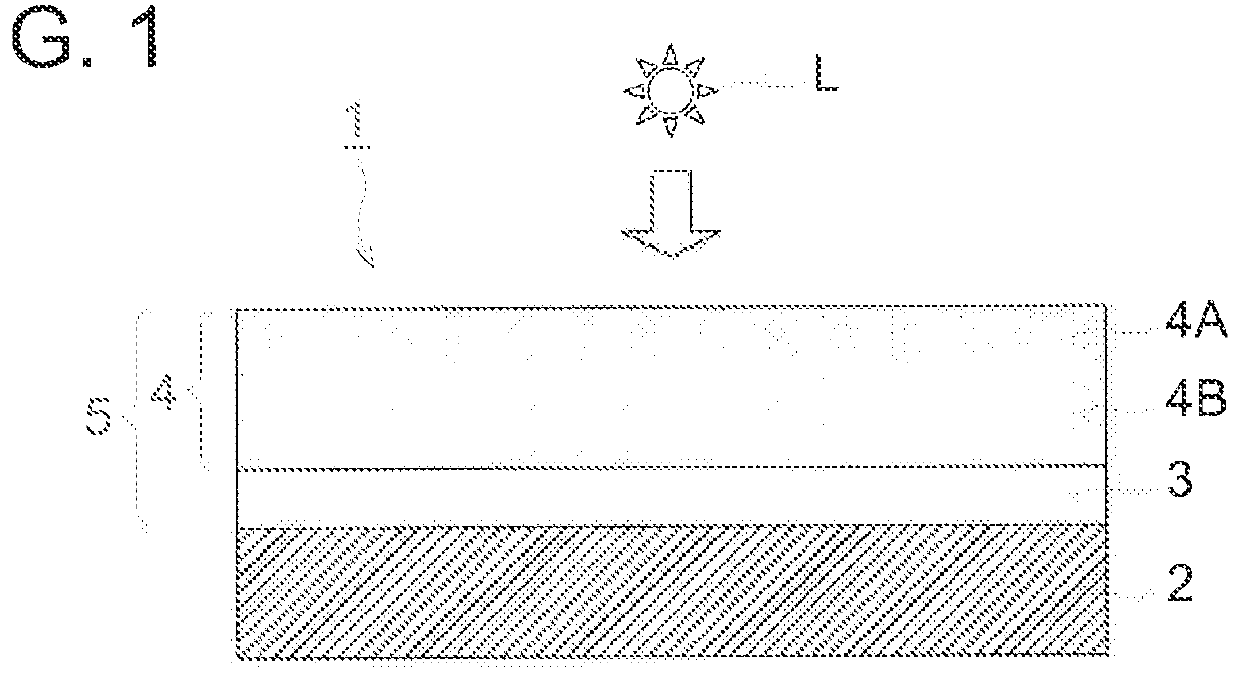
Gas barrier film, process for production of gas barrier film, and electronic device
a technology of gas barrier film and gas barrier film, which is applied in the field of gas, can solve the problems of insufficient flexibility, reduced effective area as a final product, and weakened cutting edge portion of the film, and achieves the effects of bending resistance and smoothness, good barrier property, and appropriate cutting process aptitud
- Summary
- Abstract
- Description
- Claims
- Application Information
AI Technical Summary
Benefits of technology
Problems solved by technology
Method used
Image

Examples
example 1
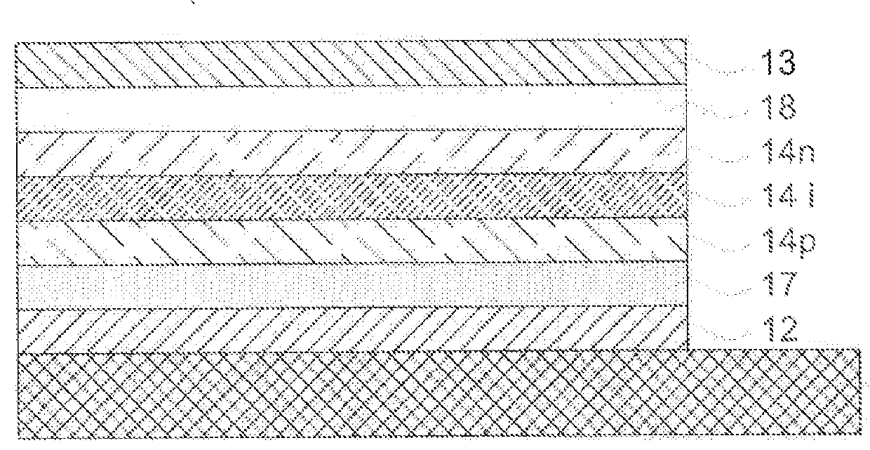
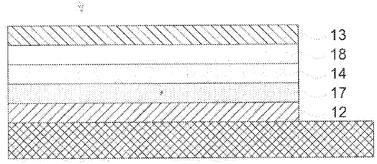
Preparation of Sample 1 (Gas Barrier Film)
[Formation of First Barrier Layer 1]
[0385]By using an atmospheric pressure plasma film forming apparatus (described in FIG. 3 of JP-A No. 2008-56967, Atmospheric pressure plasma CVD apparatus of roll to roll type), a first barrier layer 1 (100 nm) was formed with an atmospheric pressure plasma method on a transparent resin substrate (polyethylene terephthalate (PET) film provided with a clear hard coat layer (CHC) having a thickness of PET of 125 μm and a thickness of CMC of 6 μm, made by Kimoto Co., Ltd.). The thin film forming conditions used are shown below.
(Mixed Gas Composition)
[0386]Discharge gas: nitrogen gas, 94.9 volume %
[0387]Thin film forming gas: tetraethoxysilane, 0.1 volume %
[0388]Additive gas: oxygen gas, 5.0 volume %
(Film Forming Conditions)
[0389]Type of power source: PHF-6, 100 kHz (continuous mode), made by HAIDEN LABORATORY, Co., Ltd.
[0390]Frequency: 100 kHz
[0391]Output density: 10 W / cm2
[0392]Electrode temperature: 120° C...
example 2
Preparation of Electronic Device
[0580]On each of the gas barrier films 1 to 17 prepared in Example 1 was provided with a first electrode by patterning an indium tin oxide (ITO) transparent conductive film accumulated to a thickness of 150 nm (of which sheet resistance was 10Ω / □) to a width of 2 mm via a commonly used photolithographic technique and a wet etching technique. The patterned first electrode was washed via sequential steps of ultrasonic washing using a surfactant and ultra pure water and ultrasonic washing using ultra pure water, followed by drying under a nitrogen flow, and, finally, cleaned via ultraviolet / ozone cleaning.
[0581]On the transparent substrate, Baytron P4083 (produced by Starck-V TECH, Inc.) was applied and then dried to obtain a layer thickness of 30 nm, subsequently, the layer was subjected to a heat treatment at 150° C. for 30 minutes to form a hole transport layer.
[0582]After that, each substrate was carried in into a nitrogen chamber and preparation was...
PUM
| Property | Measurement | Unit |
|---|---|---|
| thickness | aaaaa | aaaaa |
| height Rt(p) | aaaaa | aaaaa |
| thickness | aaaaa | aaaaa |
Abstract
Description
Claims
Application Information
 - R&D Engineer
- R&D Manager
- IP Professional
- Industry Leading Data Capabilities
- Powerful AI technology
- Patent DNA Extraction
Browse by: Latest US Patents, China's latest patents, Technical Efficacy Thesaurus, Application Domain, Technology Topic.
© 2024 PatSnap. All rights reserved.Legal|Privacy policy|Modern Slavery Act Transparency Statement|Sitemap