Supercharge Your Innovation With Domain-Expert AI Agents!

Optical printed circuit board

a printed circuit board and optical technology, applied in the field of optical printed circuit boards, can solve the problems of difficult to precisely position the light waveguides, uneven surface of the printed circuit layer,

Inactive Publication Date: 2016-07-19
HON HAI PRECISION IND CO LTD
View PDF8 Cites 0 Cited by
  • Summary
  • Abstract
  • Description
  • Claims
  • Application Information

AI Technical Summary

Benefits of technology

The present patent relates to an optical printed circuit board (PCB) that addresses the limitations of current optical PCBs. The technical effect of the patent is to provide an optical PCB that can accurately position light waveguides, even if the surface of the PCB is uneven due to conductive traces. This is achieved by using an adjusting sheet between the substrate and the solder resist layer covering the conductive traces, which can adjust the position of the light waveguide to ensure a flat surface for accurate mounting.

Problems solved by technology

The surface of the printed circuit layer will be uneven because of conductive traces.
As such, the surface of the solder resist layer, on which the light waveguides are positioned, will not be flat, which makes it difficult to precisely position the light waveguides.

Method used


Image

  • Optical printed circuit board
  • Optical printed circuit board
  • Optical printed circuit board

Examples


Embodiment Construction

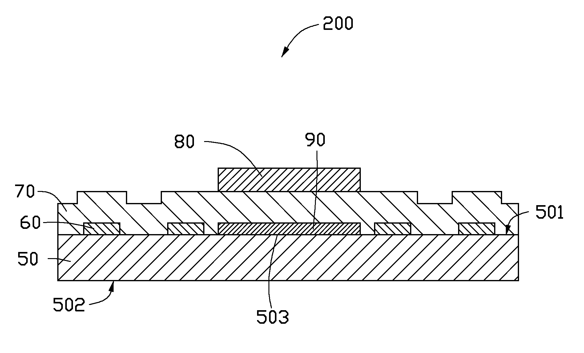
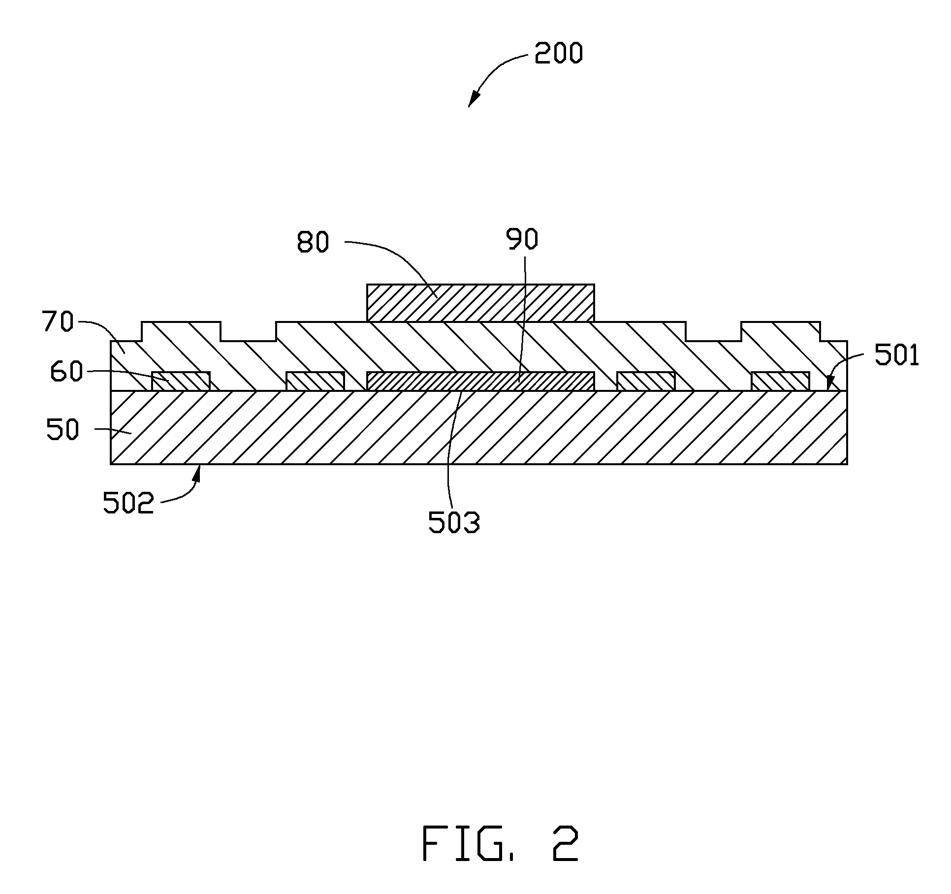
[0009]FIG. 1 shows an optical PCB 100 according to a first exemplary embodiment. The optical PCB 100 includes a substrate 10, a number of conductive traces 20 formed on the substrate 10, a solder resist layer 30 formed on the substrate 10 and covering the conductive traces 20, and a light waveguide 40 positioned on a surface of the solder resist layer 30 opposite to the conductive traces 20.

[0010]The substrate 10 includes a first surface 101 and an opposite second surface 102. The first surface 101 includes a first area 103 substantially coinciding with an orthogonal projection of the light waveguide 40 on the first surface 101.

[0011]The conductive traces 20 form one or more printed circuits (not labeled) of the optical PCB 100. The conductive traces 20 are only formed outside of the first area 103 on the first surface 101. In other words, the first area 103 is kept clear of the conductive traces 20 to provide a flat expanse to more stably precisely mount the light waveguide 40. The...


PUM


Abstract

An optical PCB includes a substrate, conductive traces, a solder resist layer, and a light waveguide. The substrate includes a surface. The surface includes a flat area. The conductive traces are formed on the surface of the substrate and only positioned outside of the flat area. The solder resist layer is formed on the substrate and covers the conductive traces. The light waveguide is positioned on the solder resist layer. An orthogonal projection of the light waveguide on the surface of the substrate coincides with the flat area.

Description

BACKGROUND[0001]1. Technical Field[0002]The present disclosure relates to an optical printed circuit board (PCB).[0003]2. Description of Related Art[0004]An optical PCB is a PCB that can transmit information using optical signals. Many optical PCBs include an insulated substrate, a printed circuit layer formed on a surface of the substrate, a solder resist layer applied to the printed circuit layer, and light waveguides positioned on the solder resist layer. The surface of the printed circuit layer will be uneven because of conductive traces. As such, the surface of the solder resist layer, on which the light waveguides are positioned, will not be flat, which makes it difficult to precisely position the light waveguides.[0005]What is needed therefore is an optical PCB addressing the limitations described.BRIEF DESCRIPTION OF THE DRAWINGS[0006]The components of the drawings are not necessarily drawn to scale, the emphasis instead being placed upon clearly illustrating the principles ...

Claims


Application Information

Patent Timeline
Patent Type & Authority Patents(United States)
IPC IPC(8): G02B6/10G02B6/122G02B6/43
CPCG02B6/10G02B6/122G02B6/43
Inventor WU, KAI-WEN
Owner HON HAI PRECISION IND CO LTD
Features
  • R&D
  • Intellectual Property
  • Life Sciences
  • Materials
  • Tech Scout
  • Unparalleled Data Quality
  • Higher Quality Content
  • 60% Fewer Hallucinations
Learn More