Method of forming mask pattern and method of manufacturing semiconductor device

a semiconductor device and mask pattern technology, applied in the direction of electrical equipment, basic electric elements, electric discharge tubes, etc., can solve the problems of reducing the flatness of the sidewall of the line portion or the flatness of the silicon oxide film covering the sidewall of the line portion, and the mask pattern made up of the remaining sidewall portions cannot have a uniform and highly precise shape,

Inactive Publication Date: 2013-01-24
TOKYO ELECTRON LTD
View PDF9 Cites 275 Cited by
  • Summary
  • Abstract
  • Description
  • Claims
  • Application Information

AI Technical Summary

Benefits of technology

[0008]In view of the above, the invention provides a mask pattern forming method and a semiconductor device manufacturing method, which are capable of preventing a core member made up of a resist film from being deformed when a silicon oxide film for forming sidewall portions is formed and the silicon oxide film thus formed is etched back in case of forming a fine mask pattern using a SWP method.
[0010]In accordance with the invention, it is possible to prevent a core member made up of a resist film from being deformed when a silicon oxide film for forming the sidewall portions is formed and the silicon oxide film thus formed is etched back in forming a fine mask pattern using a SWP method.

Problems solved by technology

However, the above-described SWP method of forming the fine mask pattern having a resolution lower than a resolution limit of the photolithography technique has the following problem.
Since the resist film exposed to plasma reacts with the plasma, a surface of the line portion may be roughened or deformed, which may result in deterioration of flatness of a sidewalls of the line portion or reduction of a line width of the line portion.
If the flatness of the sidewalls of the line portion is deteriorated, the silicon oxide film covering the sides of the line portion cannot be formed with high flatness.
Thus, the mask pattern made up of the remaining sidewall portions cannot have a uniform and highly precise shape.
In addition, if the line width of the line portion is reduced, the sidewall portions covering the sides of the line portion are likely to be inclined or collapsed in one direction.
In either case, since the sidewall portions cannot have a uniform and highly precise shape, when an underlying layer is etched using the mask pattern including the sidewall portions as a mask, a shape formed by the etching cannot have uniformity and high precision.

Method used


Image

  • Method of forming mask pattern and method of manufacturing semiconductor device
  • Method of forming mask pattern and method of manufacturing semiconductor device
  • Method of forming mask pattern and method of manufacturing semiconductor device

Examples


first embodiment

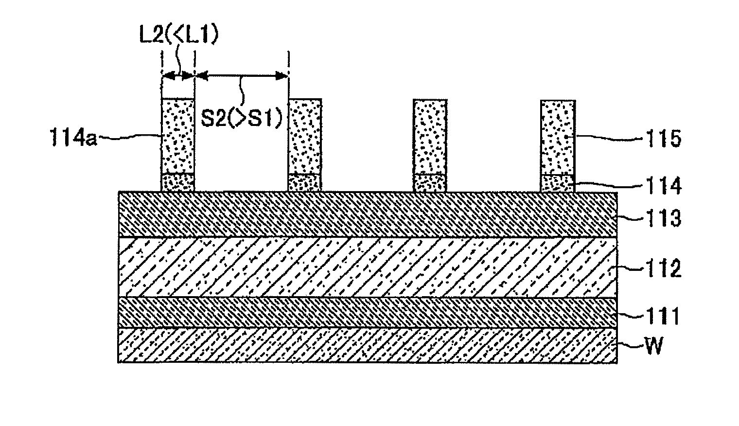
[0024]A method of forming a mask and a method of manufacturing a semiconductor device in accordance with a first embodiment of the present invention will be described below with reference to FIGS. 1 to 9.

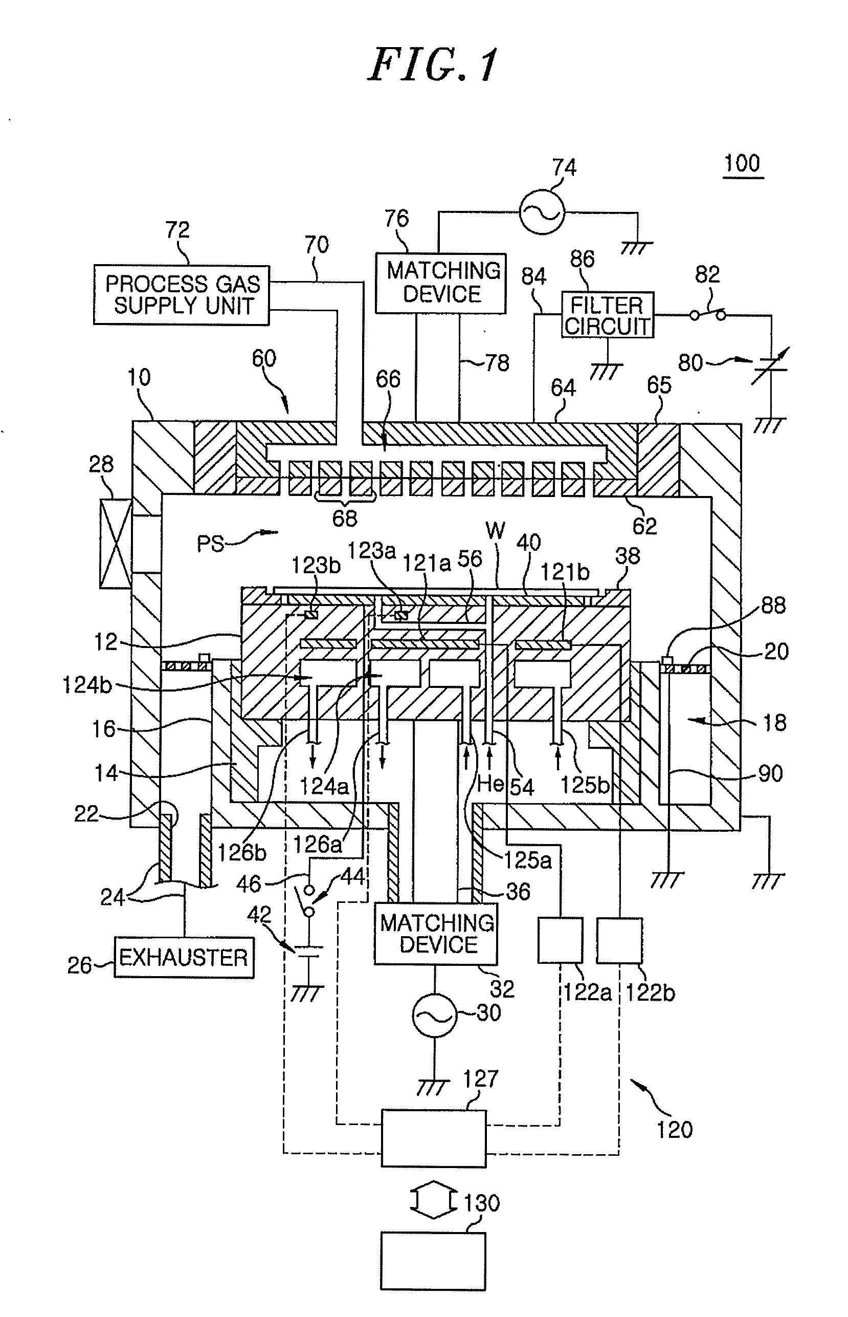
[0025]First, a plasma processing apparatus in accordance with this embodiment which is adapted for practice of the method of forming a mask and the method of manufacturing a semiconductor device in accordance with the first embodiment of the present invention will be described.

[0026]Referring to FIG. 1, a plasma processing apparatus 100 is implemented with a capacitive coupling type plasma etching apparatus and has a cylindrical chamber (process chamber) 10 made of metal such as aluminum, stainless steel or the like. The chamber is grounded.

[0027]Within the chamber is horizontally placed a disc-like susceptor 12 serving as a lower electrode, on which a semiconductor wafer W (hereinafter abbreviated as a “wafer W”) is mounted as a substrate to be processed, for example. The susceptor...

example 1

[0122]In Example 1, the steps S11 to S18 in FIG. 3 were performed. Conditions of the steps S13, S14 and S16 to S18 in Example 1 are as follows.

(A) First Pattern Forming Step S13

[0123]Internal pressure of film forming apparatus: 800 mTorr

[0124]Power of high frequency power supply (40 MHz / 13 MHz): 200 / 0 W

[0125]Voltage of upper electrode: −600 V

[0126]Wafer temperature (Center / perimeter): 30 / 30° C.

[0127]Flow rate of process gas (CF4 / O2 / Ar): 150 / 50 / 1000 sccm

[0128]Process time: 30 sec

(B) Irradiation Step S14

[0129]Internal pressure of film forming apparatus: 100 mTorr

[0130]Power of high frequency power supply (40 MHz / 13 MHz): 500 / 0 W

[0131]Voltage of upper electrode: −900 V

[0132]Wafer temperature (Center / perimeter): 30 / 30° C.

[0133]Flow rate of process gas (H2 / Ar): 450 / 450 sccm

[0134]Process time: 10 sec

(C) Etch Back Step S16

[0135]Internal pressure of film forming apparatus: 30 mTorr

[0136]Power of high frequency power supply (40 MHz / 13 MHz): 500 / 100 W

[0137]Voltage of upper electrode: 300 V

[01...

example 2

[0153]In Example 2, the steps S11 to S18 in FIG. 8 were performed. Conditions of the steps S14 and S16 to S18 in Example 2 are the same as Example 1. Conditions of the step S13′ in Example 2 are as follows.

(F) First Pattern Forming Step S13′

[0154]Internal pressure of film forming apparatus: 800 mTorr

[0155]Power of high frequency power supply (40 MHz / 13 MHz): 200 / 0 W

[0156]Voltage of upper electrode: 0 V

[0157]Wafer temperature (Center / perimeter): 30 / 30° C.

[0158]Flow rate of process gas (CF4 / O2 / Ar): 150 / 20 / 1000 sccm

[0159]Process time: 55 sec


PUM


Abstract

A method of forming a mask pattern includes a first pattern forming step of etching an anti-reflection coating film by using as a mask a first line portion made up of a photo resist film formed on the anti-reflection film to form a pattern including a second line portion made up of the photo resist film and the anti-reflection film; an irradiation step of irradiating the photo resist film with electrons; a silicon oxide film forming step to cover the second line portion isotropically; and an etch back step of etching back the silicon oxide film such that the silicon oxide film is removed from the top of the second line portion as sidewalls of the second line portion. The method further includes a second pattern forming step of ashing the second line portion to form a mask pattern including a third line portion made up of the silicon oxide film and remains.

Description

FIELD OF THE INVENTION[0001]The present invention relates to a method of forming a mask pattern and a method of manufacturing a semiconductor device.BACKGROUND OF THE INVENTION[0002]With high integration of semiconductor devices, dimensions of wirings and isolation regions have a tendency of miniaturization. Such a miniaturized pattern is formed by providing a pattern in which line portions formed of a photo resist film (hereinafter abbreviated as a “resist film”) are arranged at predetermined intervals by using a photolithography technique, and etching a film to be etched using the formed pattern as a mask pattern. The recent miniaturization of semiconductor devices gets up to requirement of dimension of less than resolution limit of the photolithography technique.[0003]A so-called “double patterning” method is a method of forming a fine mask pattern having a dimension of less than resolution limit of the photolithography technique. The double patterning method includes two steps: ...

Claims


Application Information

Patent Timeline
Patent Type & Authority Applications(United States)
IPC IPC(8): H01L21/306
CPCH01J37/32091H01L21/02164H01L21/02274H01L21/0273H01L21/0337H01L21/0338H01L21/31138H01L21/32139H01L21/02211H01L21/0228H01L21/31116
Inventor YAEGASHI, HIDETAMIIGARASHI, YOSHIKINARISHIGE, KAZUKIMUKAWA, TAKAHITO
Owner TOKYO ELECTRON LTD
Why Eureka
Try Eureka