Method of inspecting pixel array substrate and apparatus for inspecting pixel array substrate

a technology inspection method, which is applied in the direction of instruments, static indicating devices, etc., can solve the problems of difficult control difficult alignment of probes on fixtures with pixel array substrates, and easy scratching etc., and achieves the effect of easy inspection of pixel array substrates

Active Publication Date: 2016-11-08
E INK HLDG INC
View PDF14 Cites 0 Cited by
  • Summary
  • Abstract
  • Description
  • Claims
  • Application Information

AI Technical Summary

Benefits of technology

[0007]The invention provides an inspection method capable of easily inspecting a pixel array substrate.
[0008]The invention provides an inspection apparatus capable of inspecting a pixel array substrate and has a low price.
[0029]According to the foregoing, the inspection method and the inspection apparatus in the embodiments of the invention enable the photoelectric inspection device to be in contact with the to-be inspected pixel array substrate and inputs the electrical signals to the pixel array substrate and the photoelectric inspection device, and then determines whether the pixel units of the pixel array substrate are normal or not based on the optical property of the photoelectric inspection device. The inspection apparatus in the embodiments of the invention has a simple structure, low manufacturing cost, and may easily determine defects of the pixel array substrate. The defects of the pixel array substrate may be easily determined by using the inspection method and the inspection apparatus described in the embodiments of the invention, and subsequent processing materials and time may be avoided from being wasted, thereby achieving a purpose of reducing the costs.

Problems solved by technology

In the conventional techniques, a fixture has to be changed when inspecting of the pixel array substrate, and a probe on the fixture is not easily aligned with the pixel array substrate, or a gap between a modulator used for inspecting the pixel array substrate and the pixel array substrate is difficult to be controlled, and the pixel array substrate is easily be scratched.
In other words, the conventional inspection method is complicated, and the conventional inspection apparatus has a complex structure and is expensive.

Method used


Image

  • Method of inspecting pixel array substrate and apparatus for inspecting pixel array substrate
  • Method of inspecting pixel array substrate and apparatus for inspecting pixel array substrate
  • Method of inspecting pixel array substrate and apparatus for inspecting pixel array substrate

Examples


Embodiment Construction

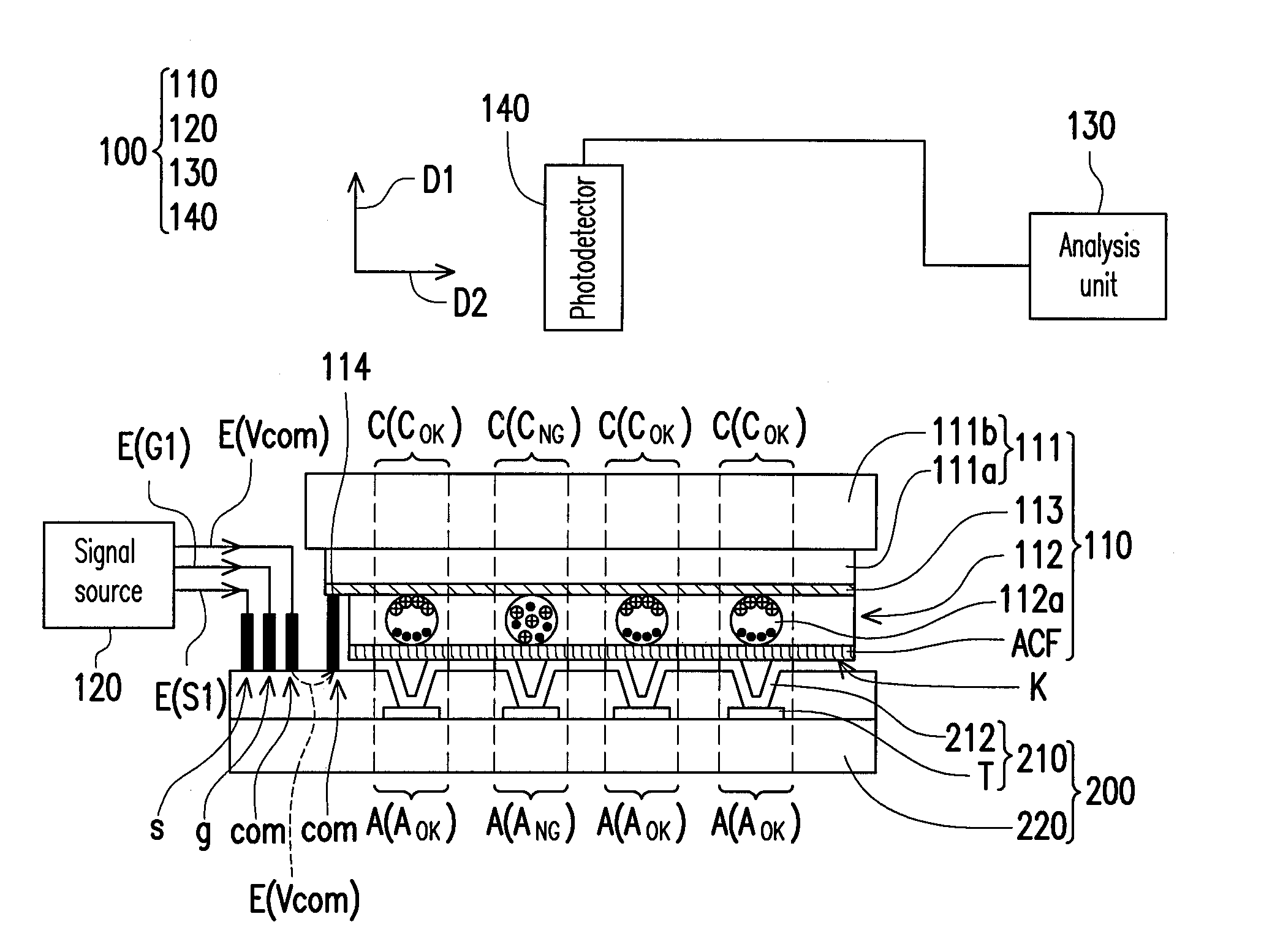
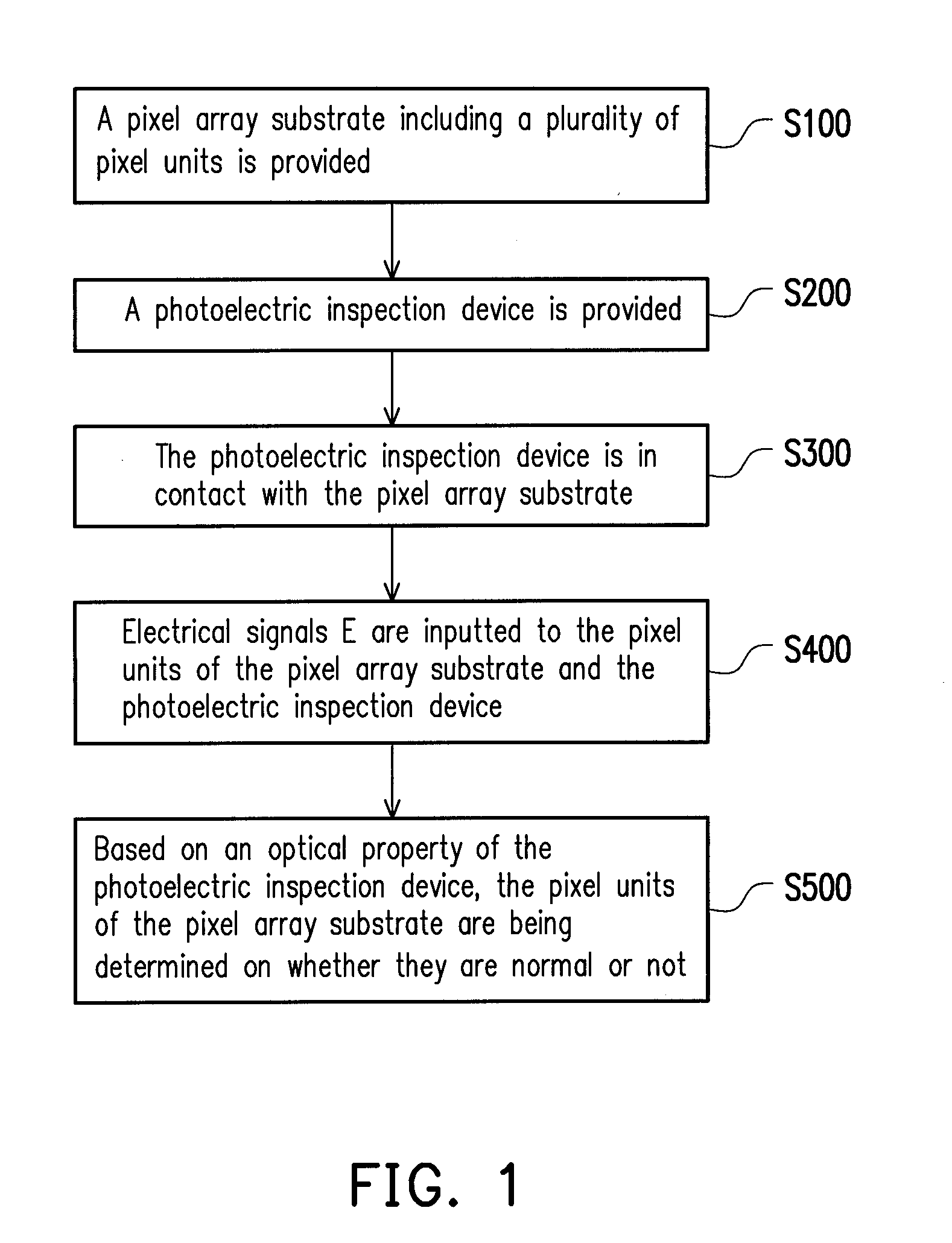
[0036]FIG. 1 is a schematic flow diagram illustrating an inspection method according to an embodiment of the invention. FIG. 2 is a schematic diagram illustrating an inspection apparatus according to an embodiment of the invention. In particular, the inspection apparatus 100 of FIG. 2 can specifically implement the inspection method of FIG. 1. The inspection method and the inspection apparatus 100 are to be explained in detail, along with FIG. 1 and FIG. 2, in the following.

[0037]Referring to FIG. 1 and FIG. 2, the inspection method and the inspection apparatus 100 of the present embodiment are configured to inspect a pixel array substrate 200 including a plurality of pixel units 210. Firstly, the pixel array substrate 200 including the pixel units 210 is provided (step S100). As shown in FIG. 2, in the present embodiment, the pixel array substrate 200 further includes a substrate 220, and the pixel units 210 are disposed on the substrate 220. Each of the pixel units 210 includes at...


PUM


Abstract

An inspection method including following steps is provided. A pixel array substrate including a plurality of pixel units is in contact with a photoelectric inspection device. A plurality of electrical signals is inputted to the pixel units of the pixel array substrate and the photoelectric inspection device. Based on an optical property of the photoelectric inspection device, the pixel units of the pixel array substrate are being examined on whether they are normal or not. Moreover, an inspection apparatus realizing the inspection method is also provided.

Description

CROSS-REFERENCE TO RELATED APPLICATION[0001]This application claims the priority benefit of Taiwan application serial no. 102115288, filed on Apr. 29, 2013. The entirety of the above-mentioned patent application is hereby incorporated by reference herein and made a part of this specification.BACKGROUND[0002]1. Field of the Application[0003]The invention relates to an inspection method and an inspection apparatus, and more particularly, to an inspection method for inspecting a pixel array substrate and an inspection apparatus using the same.[0004]2. Description of Related Art[0005]A display includes a pixel array substrate and an opposite substrate. In a manufacturing process of the display, the pixel array substrate and the opposite substrate are respectively manufactured. Then, the pixel array substrate and the opposite substrate are assembled in a group to complete the display. In general, the pixel array substrate is inspected before the pixel array substrate and the opposite sub...

Claims


Application Information

Patent Timeline
Patent Type & Authority Patents(United States)
IPC IPC(8): G09G3/00G09G3/20G09G3/34
CPCG09G3/006G09G3/20G09G3/344G09G2300/0847G09G2360/145
Inventor LIU, CHUAN-FENGHUANG, JEN-SHIUNHUANG, PEI-LINLI, SHI-LINTSAI, CHEN-FACHANG, YUNG-SHENG
Owner E INK HLDG INC
Why Eureka
Try Eureka