

Semiconductor memory device for performing refresh operation and semiconductor memory system including the same
a memory device and memory technology, applied in the field of semiconductor memory devices, can solve the problems of cell capacitor discharged from the discharged cell capacitor unintentionally becoming charged, the charge stored in the cell capacitor changes,
- Summary
- Abstract
- Description
- Claims
- Application Information
AI Technical Summary
Problems solved by technology
Method used
Image


Examples
first embodiment
[0042]FIG. 1 is a block view illustrating a semiconductor memory device in accordance with the present invention.
[0043]Referring to FIG. 1, the semiconductor memory device may include a word line driving unit 110, a memory cell array 120, an activation time detection unit 130, an address latch unit 140, and an address output unit 150.
[0044]The word line driving unit 110 may receive an external address signal ADD inputted during a read / write operation, and activate a target word line corresponding to the address signal ADD among a plurality of word lines WL. The word line driving unit 110 may receive a neighboring word line address signal T_ADD during a refresh operation, and activate a neighboring word line corresponding to the neighboring word line address signal T_ADD, which will be described later on.
[0045]The memory cell array 120 may store data and include a plurality of word lines WL. Each of the word lines WL may be coupled with a plurality of memory cells. Each of the memory...
second embodiment
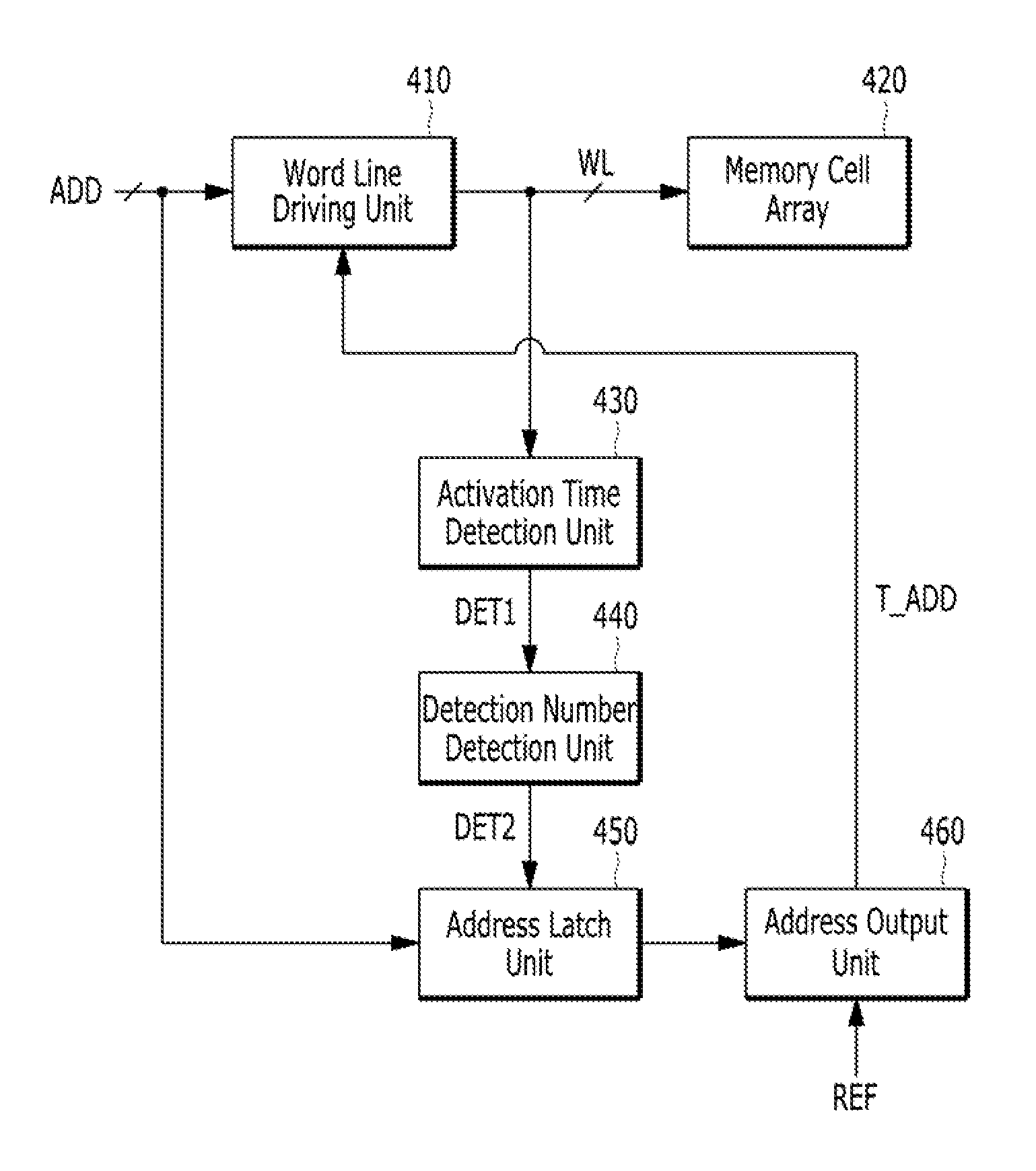
[0066]FIG. 4 is a block view illustrating a semiconductor memory device in accordance with the present invention.
[0067]The activation of a word line is closely related to an active operation because the word line is activated according to an address signal that is inputted together with an active signal, which means that activation numbers of the target word line may matter as well as the single activation time of the target word line. When the target word line is shortly activated each time but activated multiple times in response to plural active signals, the coupling effect on the neighboring word lines from the shortly activated target word line may still be a concern despite of the refresh operation of the neighboring word lines according to the long activated target word line in response to a single active signal. FIG. 4 shows a solution to this concern.
[0068]Referring to FIG. 4, the semiconductor memory device may include a word line driving unit 410, a memory cell array 420,...
third embodiment
[0082]FIG. 7 is a block view illustrating a semiconductor memory device in accordance with the present invention.
[0083]The semiconductor memory device shown in FIG. 7 may be the same as the semiconductor memory device described with reference to FIGS. 1 to 3 except for a reset control unit 710 and an activation time detection unit 720. Hereafter, the reset control unit 710 and the activation time detection unit 720 are described.
[0084]Referring to FIG. 7, the reset control unit 710 may generate a reset signal RST for initializing a counting operation of the activation time detection unit 720 in response to an address signal ADD and an active signal ACT. This will be described later in detail with reference to FIG. 8.
[0085]The activation time detection unit 720 may detect the activation time of the target word line that is activated through a counting operation. The activation time detection unit 720 may perform the counting operation in response to the active signal ACT, and perform...
PUM
 Abstract
Description
Claims
Application Information