

Method of forming crystalline oxide semiconductor film
a technology of crystalline oxide and semiconductor film, which is applied in the direction of crystal growth process, polycrystalline material growth, chemically reactive gas, etc., can solve the problems of microscopically uneven concentration of metal atoms and oxygen atoms, and achieve good characteristics, low cost, and high reliability
- Summary
- Abstract
- Description
- Claims
- Application Information
AI Technical Summary
Benefits of technology
Problems solved by technology
Method used
Image

Examples
embodiment 1
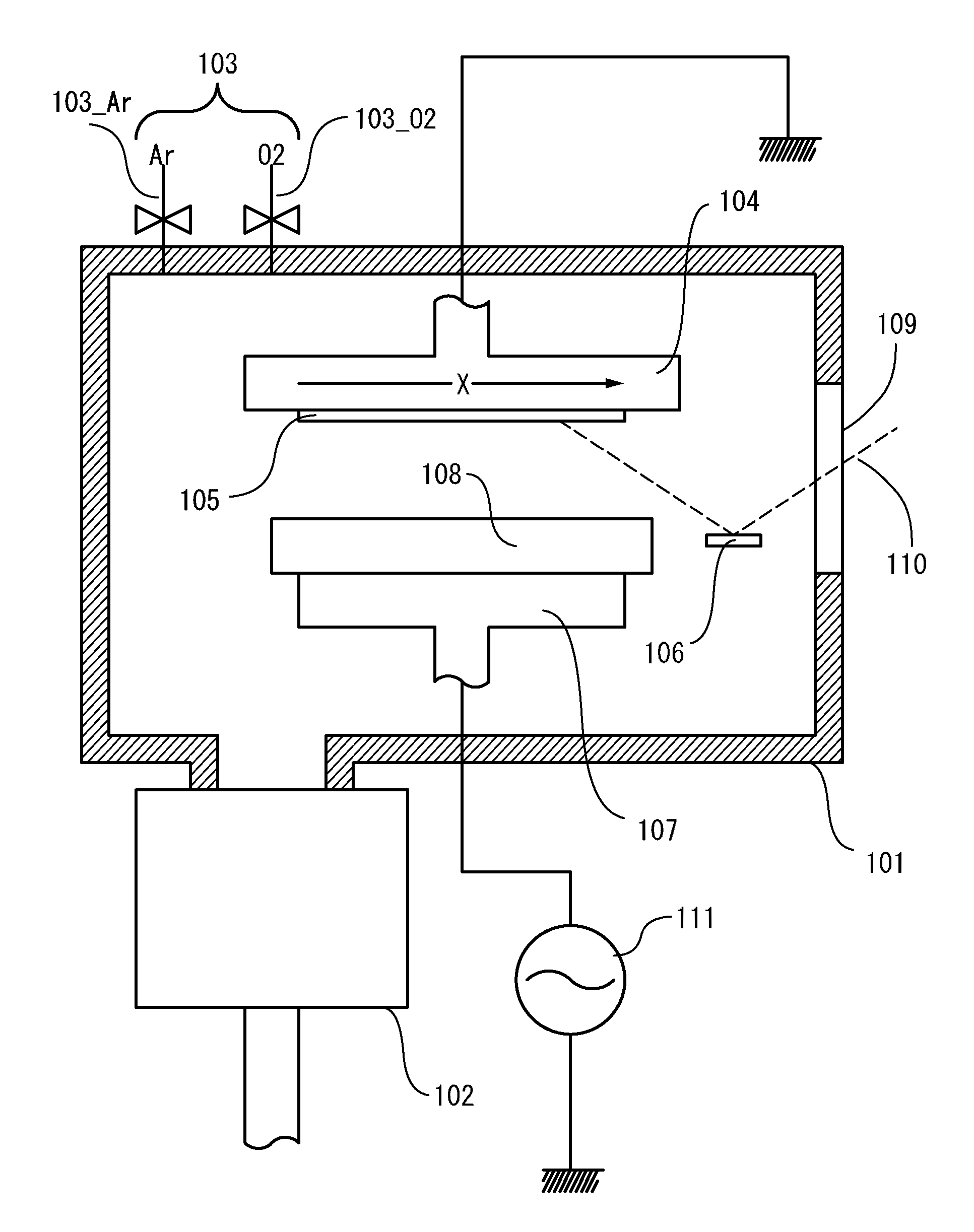
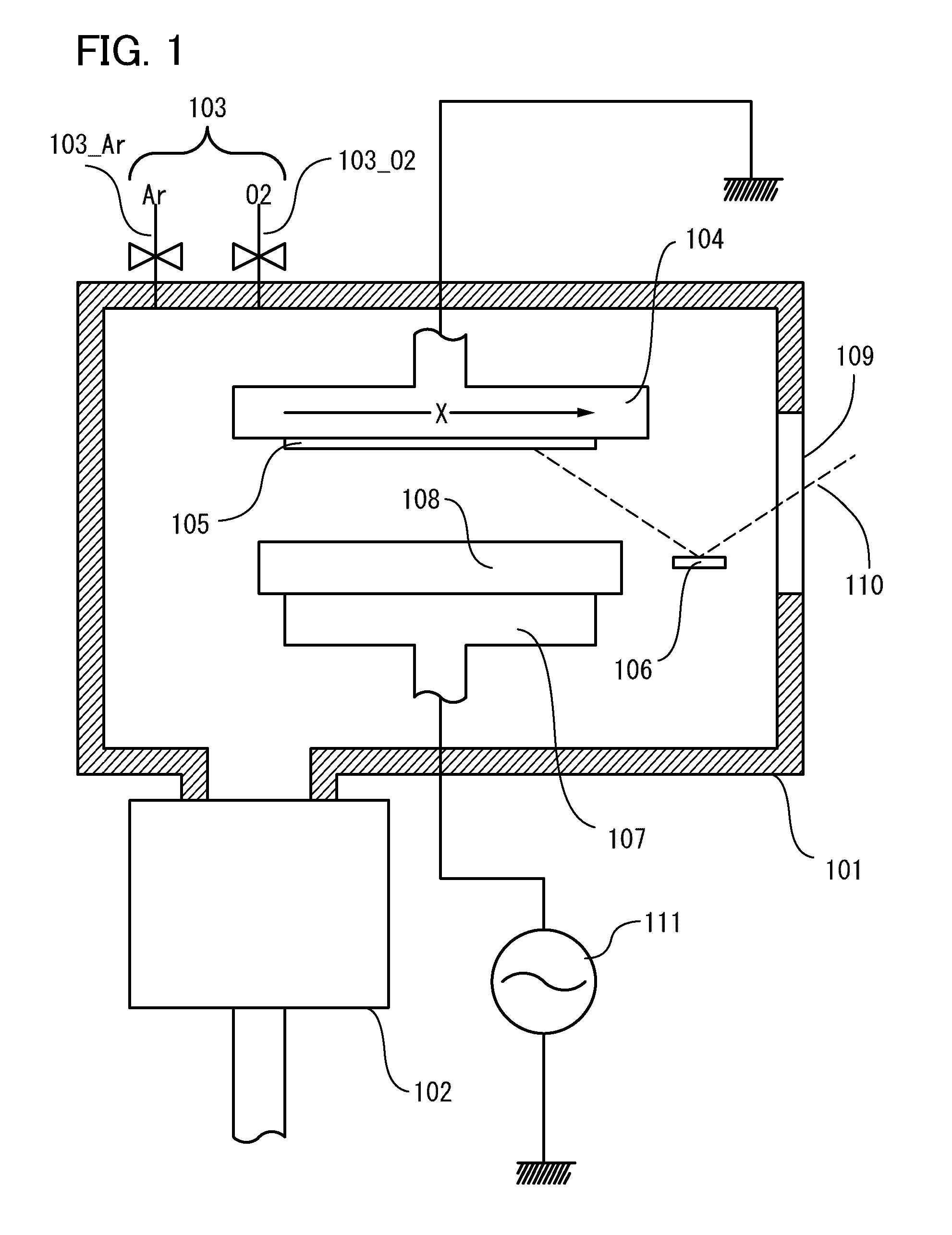
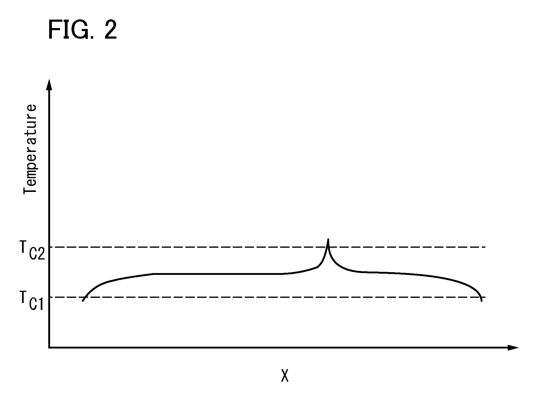
[0051]In this embodiment, an apparatus for forming an oxide semiconductor film with high crystallinity is described with reference to FIG. 1 and FIG. 2. In FIG. 1, an outline of a film formation apparatus described in this embodiment is illustrated. The oxide semiconductor film is formed by a sputtering method with the use of the film formation apparatus.
[0052]The film formation apparatus includes a film formation chamber 101, an exhaust system 102, a gas system 103 (including a line for argon 103_Ar and a line for oxygen 103_O2 here), a substrate holder 104, an optical system 106, a target holder 107, a window 109, and a power source 111.
[0053]The exhaust system 102 includes a vacuum pump such as a turbo molecular pump, and the exhaust system 102 is used for evacuating the film formation chamber 101 to a vacuum level or keeping the pressure in the film formation chamber 101 at a pressure appropriate for film formation. In particular, the characteristics of an oxide semiconductor ar...
embodiment 2
[0072]In this embodiment, an example of manufacturing a display device including a transistor with the use of an oxide semiconductor formed using the above-described film formation device is described. FIGS. 3A to 3E are cross-sectional views illustrating a process of manufacturing the display device of this embodiment. The transistor described in this embodiment has a top-gate structure in which a gate electrode is located on the side of a semiconductor layer which is opposite to the substrate, and a top-contact structure in which a source electrode and a drain electrode are in contact with a top surface of a semiconductor layer.
[0073]The outline of a manufacturing process will be described below. As illustrated in FIG. 3A, a base insulating film 202 is formed over a substrate 201 having an insulating surface.
[0074]There is no particular limitation on a substrate which can be used for the substrate 201; however, the substrate needs to have an insulating surface. For example, a glas...
embodiment 3
[0112]This embodiment will be described with reference to FIGS. 4A to 4C and FIGS. 6A to 6D. FIGS. 6A to 6C are top views, and FIGS. 4A to 4C are cross-sectional views corresponding to FIGS. 6A to 6C. FIGS. 4A to 4C are cross-sectional views taken along dot-dashed line A-B in FIGS. 6A to 6C. This embodiment shows an example of a hybrid type semiconductor device in which a semiconductor circuit using an oxide semiconductor is formed over a semiconductor circuit formed using a single crystal semiconductor substrate.
[0113]The semiconductor device formed in this embodiment is a semiconductor memory device whose circuit diagram is illustrated in FIG. 6D. Two memory elements are illustrated on the left and the right in FIG. 6D. The memory elements each include a first transistor including an oxide semiconductor, a second transistor including a single crystal semiconductor, and a capacitor. A source of the first transistor and a gate of the second transistor (304a and 304b) are connected t...
PUM
| Property | Measurement | Unit |
|---|---|---|
| length | aaaaa | aaaaa |
| temperature | aaaaa | aaaaa |
| temperature | aaaaa | aaaaa |
Abstract
Description
Claims
Application Information