

Semiconductor device including first interface and second interface as an upper surface of a convex protruded from first interface and manufacturing device thereof
a manufacturing device and semiconductor technology, applied in the direction of semiconductor devices, basic electric elements, electrical appliances, etc., can solve the problems of increasing on resistance, deteriorating electrical properties of a previously formed n-type semiconductor layer, and complicated manufacturing process, so as to relieve potential crowding, and improve the crystal quality of the second n-type semiconductor layer
- Summary
- Abstract
- Description
- Claims
- Application Information
AI Technical Summary
Benefits of technology
Problems solved by technology
Method used
Image

Examples
first embodiment
A. First Embodiment
[0098]A-1. Structure of Semiconductor Device
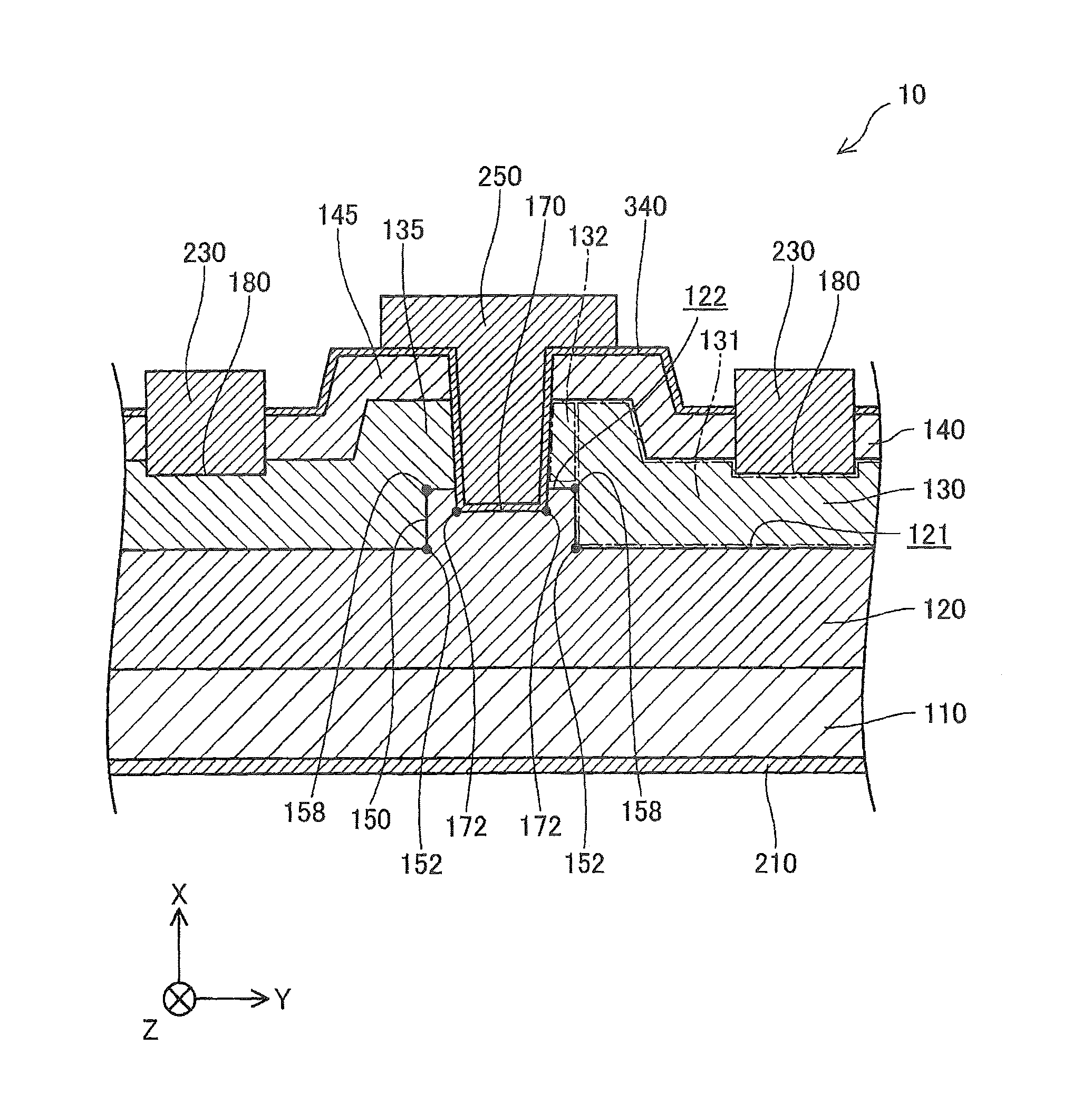
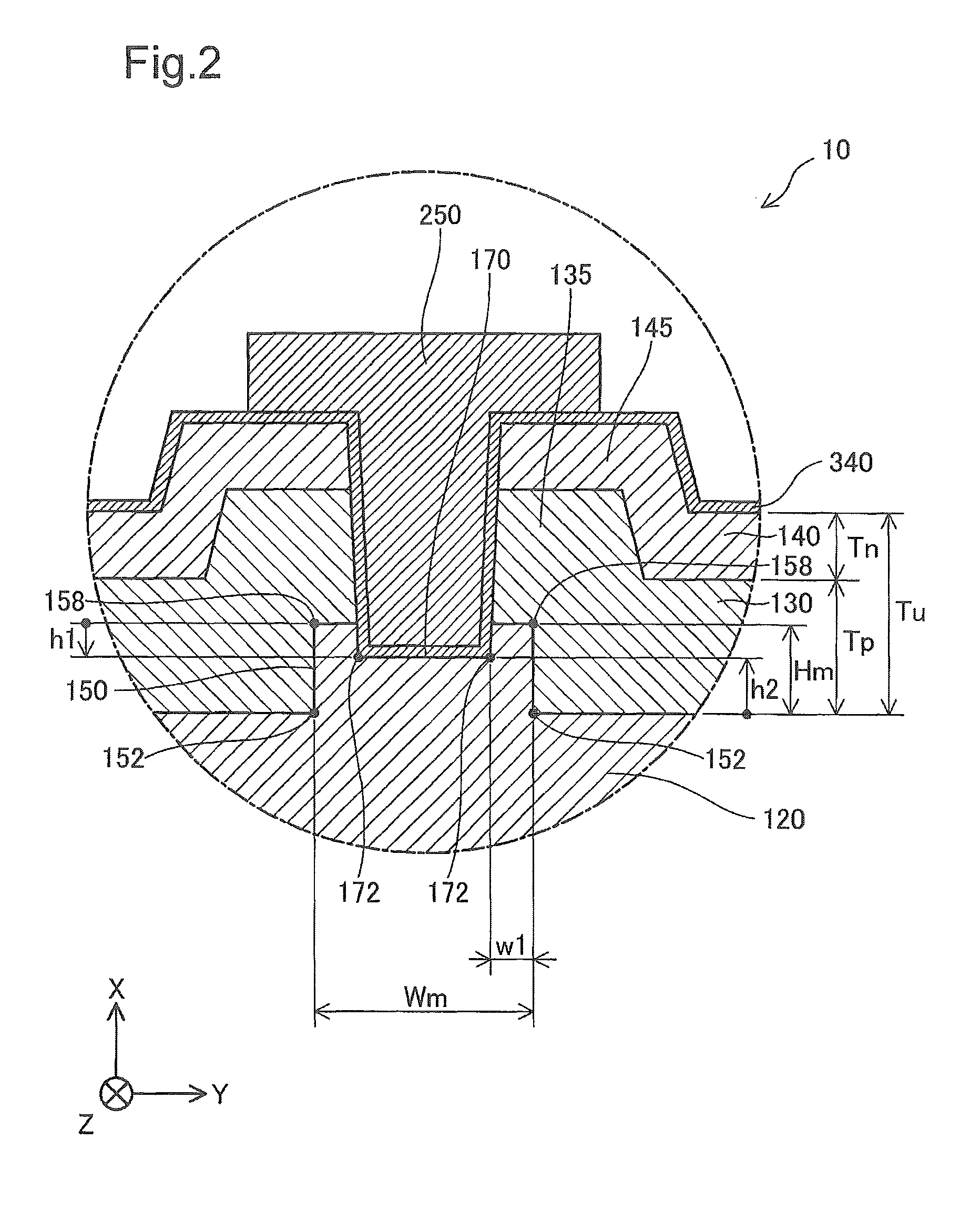
[0099]FIG. 1 is a cross sectional view schematically illustrating the structure of a semiconductor device 10 according to a first embodiment. The semiconductor device 10 is a GaN-based semiconductor device made by using gallium nitride (GaN). According to this embodiment, the semiconductor device 10 is a trench gate MOSFET (Metal-Oxide-Semiconductor Field-Effect Transistor) used for power control and is also called power device.
[0100]The semiconductor device 10 includes a substrate 110, an n-type semiconductor layer 120, a p-type semiconductor layer 130, an n-type semiconductor layer 140, electrodes 210, 230 and 250, and an insulating film 340. A trench 170 and recesses 180 are formed in the semiconductor device 10. The semiconductor device 10 has the stacked structure where the n-type semiconductor layer 120, the p-type semiconductor layer 130 and the n-type semiconductor layer 140 are stacked sequentially. The semicond...
second embodiment
B. Second Embodiment
[0155]FIG. 11 is a cross sectional view schematically illustrating the structure of a semiconductor device 12 according to a second embodiment. XYZ axes are shown in FIG. 11 in the same manner as FIG. 1. The semiconductor device 12 of the second embodiment is similar to the semiconductor device 10 of the first embodiment, except addition of another semiconductor layer 125.
[0156]The semiconductor layer 125 is a semiconductor layer placed between the n-type semiconductor layer 120 and the p-type semiconductor layer 130 and may be regarded as part of the n-type semiconductor layer 120. According to this embodiment, the semiconductor layer 125 of the semiconductor device 12 is a third n-type semiconductor layer having the lower donor concentration than that of the p-type semiconductor layer 130. According to another embodiment, the semiconductor layer 125 may be an intrinsic semiconductor layer (undoped semiconductor layer) having the lower donor concentration than t...
third embodiment
C. Third Embodiment
[0160]FIG. 12 is a cross sectional view schematically illustrating the structure of a semiconductor device 13 according to a third embodiment. XYZ axes are shown in FIG. 12 in the same manner as FIG. 1. The semiconductor device 13 of the third embodiment is similar to the semiconductor device 10 of the first embodiment, except replacement of the electrode 230 with an electrode 232 suitable for the p-type semiconductor layer 130 and an electrode 234 suitable for the n-type semiconductor layer 140.
[0161]According to this embodiment, the electrode 232 is an electrode made of palladium (Pd). According to this embodiment, the electrode 234 is formed by stacking a layer made of aluminum (Al) on a layer made of titanium (Ti) and firing the stacked layers.
[0162]The third embodiment described above improves the electrical properties of the semiconductor device 13, like the first embodiment.
PUM
 Abstract
Description
Claims
Application Information