
Air gap spacer for metal gates

a metal gate and air gap technology, applied in the field of integrated circuits, can solve the problems of paralytic capacitance, exposure and damage to high-k materials situated around metal gates, and add insulation may harm other device components,

Active Publication Date: 2017-03-28
TESSERA LLC
View PDF11 Cites 103 Cited by
  • Summary
  • Abstract
  • Description
  • Claims
  • Application Information

AI Technical Summary

Benefits of technology

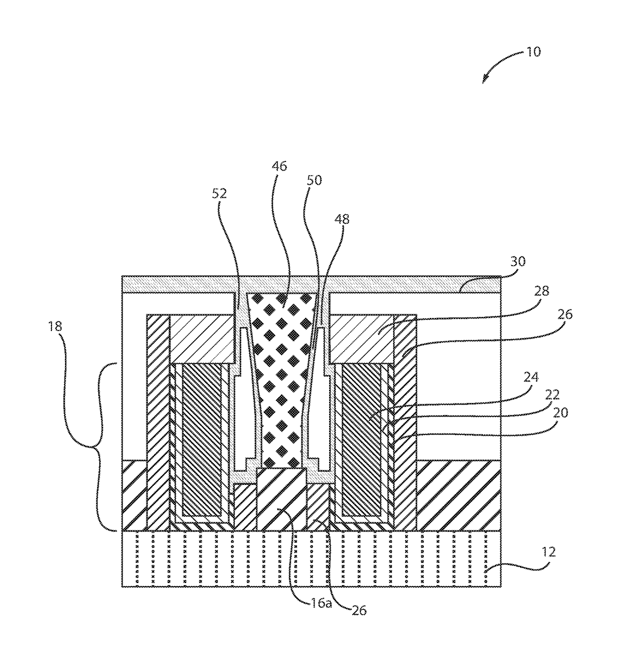
The present disclosure describes a transistor device and a method of forming a semiconductor device with air gap structures adjacent to gate structures. The technical effects of the invention improve the device's performance and reliability by reducing interference between the metal gate structures and the source, drain, and metal contacts, and by sealing air gaps between them using a conformal dielectric material layer. Additionally, the invention provides a method for forming fin structures with a simple process and at a low cost.

Problems solved by technology

Insulating selected regions of the device may reduce the parasitic capacitance, however, the processing employed to add insulation may harm other device components, such as a high dielectric constant material (high k material) that is part of a replacement metal gate structure, e.g., a gate structure formed in replacement of a sacrificial gate structure.
For example, in taking steps to improve the insulating characteristics, processing near the gate may lead to the exposure of and damage to high k material situated around the metal gates.

Method used


Image

  • Air gap spacer for metal gates
  • Air gap spacer for metal gates
  • Air gap spacer for metal gates

Examples


Embodiment Construction

[0026]Detailed embodiments of the methods and structures of the present disclosure are described herein; however, it is to be understood that the disclosed embodiments are merely illustrative of the disclosed methods and structures that may be embodied in various forms. In addition, each of the examples given in connection with the various embodiments of the disclosure are intended to be illustrative, and not restrictive. Further, the figures are not necessarily to scale, some features may be exaggerated to show details of particular components. Therefore, specific structural and functional details disclosed herein are not to be interpreted as limiting, but merely as a representative basis for teaching one skilled in the art to variously employ the methods and structures of the present disclosure.

[0027]References in the specification to “one embodiment”, “an embodiment”, “an example embodiment”, etc., indicate that the embodiment described may include a particular feature, structure...


PUM


Abstract

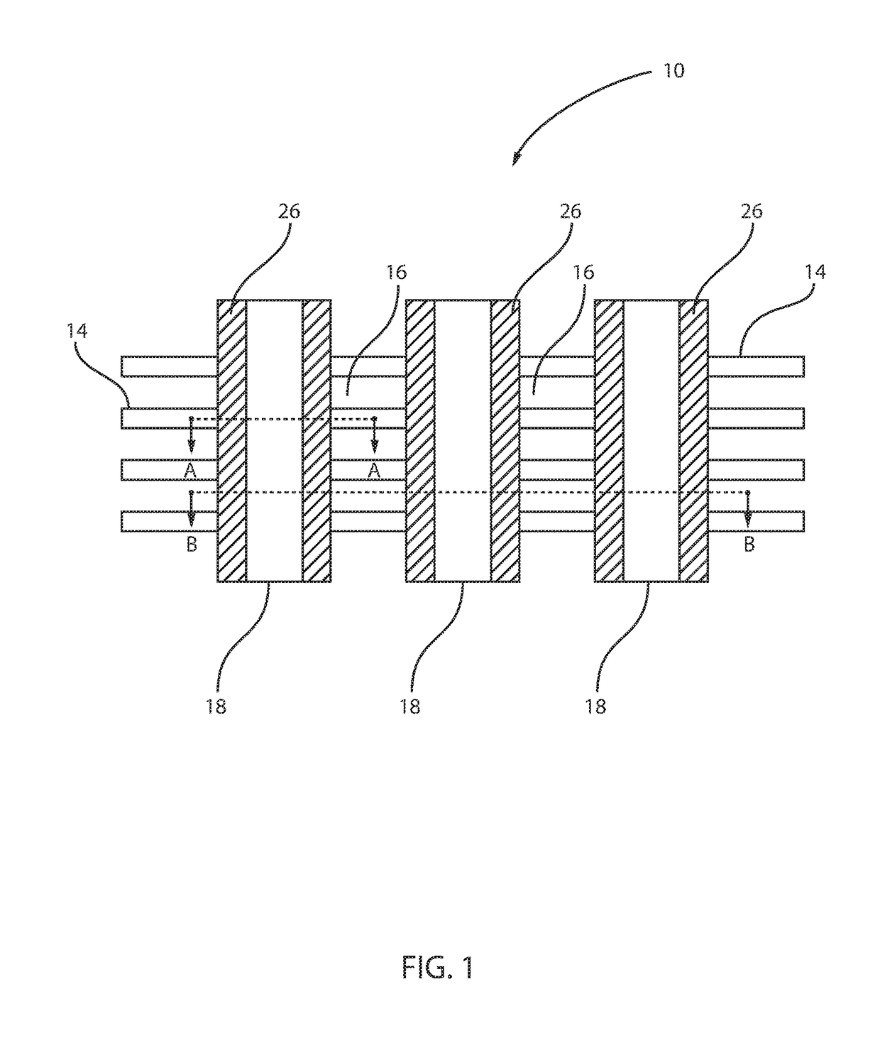
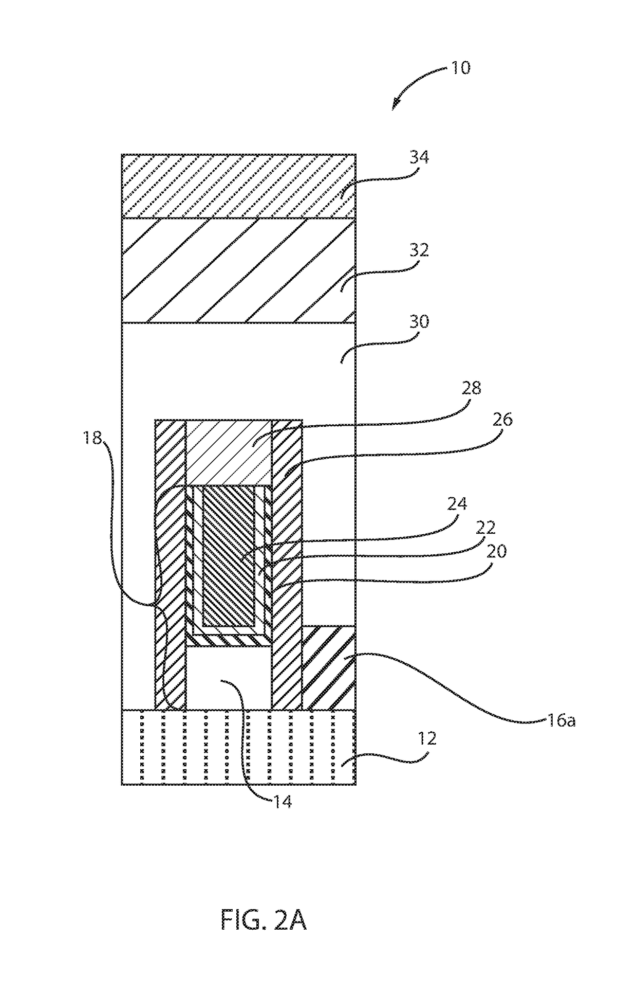
A method of forming a semiconductor device that includes forming a trench adjacent to a gate structure to expose a contact surface of one of a source region and a drain region. A sacrificial spacer may be formed on a sidewall of the trench and on a sidewall of the gate structure. A metal contact may then be formed in the trench to at least one of the source region and the drain region. The metal contact has a base width that is less than an upper surface width of the metal contact. The sacrificial spacer may be removed, and a substantially conformal dielectric material layer can be formed on sidewalls of the metal contact and the gate structure. Portions of the conformally dielectric material layer contact one another at a pinch off region to form an air gap between the metal contact and the gate structure.

Description

BACKGROUND[0001]Technical Field[0002]The present disclosure relates to integrated circuits and the fabrication thereof. More particularly, the present disclosure relates to fabricating field effect transistors (FETs) that include fins (fin-FETs) while protecting against parasitic capacitance and protecting high K materials of a replacement metal gate structure when building in insulating air gaps.[0003]Description of the Related Art[0004]Multi-gate FETs may experience in high parasitic capacitance. Insulating selected regions of the device may reduce the parasitic capacitance, however, the processing employed to add insulation may harm other device components, such as a high dielectric constant material (high k material) that is part of a replacement metal gate structure, e.g., a gate structure formed in replacement of a sacrificial gate structure. For example, in taking steps to improve the insulating characteristics, processing near the gate may lead to the exposure of and damage ...

Claims


Application Information

Patent Timeline
IPC IPC(8): H01L21/02H01L29/45H01L21/311H01L21/8234H01L29/49H01L29/08H01L29/66
CPCH01L27/0886H01L29/4966H01L29/45H01L29/6653H01L29/66795H01L21/31111H01L29/6656H01L21/02271H01L21/823431H01L21/823418H01L21/823468H01L29/66545H01L29/4991H01L21/76897H01L21/7682H01L27/088H01L2221/1063H01L21/823475H01L29/41791H01L21/76831H01L21/823481H01L29/495
Inventor BERGENDAHL, MARC A.CHENG, KANGGUOLIE, FEE LIMILLER, ERIC R.SPORRE, JOHN R.TEEHAN, SEAN
Owner TESSERA LLC
Features
  • Generate Ideas
  • Intellectual Property
  • Life Sciences
  • Materials
  • Tech Scout
  • Unparalleled Data Quality
  • Higher Quality Content
  • 60% Fewer Hallucinations
Learn More