
Method of forming graphene nanopattern by using mask formed from block copolymer

a graphene nanopattern and block copolymer technology, applied in the direction of transistors, solid-state devices, nanoinformatics, etc., can solve the problems of not being easy to realize high-performance electronic devices with graphene, and not being easy to handle graphen

Active Publication Date: 2017-08-29
SAMSUNG ELECTRONICS CO LTD
View PDF22 Cites 1 Cited by
  • Summary
  • Abstract
  • Description
  • Claims
  • Application Information

AI Technical Summary

Benefits of technology

The patent text describes methods for creating precise patterns on a graphene layer. This can be useful in creating complex structures on the layer, which can have various applications such as in electronics and sensors. The technical effects of this patent include improved precision and ease of patterning on graphene layers.

Problems solved by technology

However, it is not easy to handle graphene and to process (e.g., pattern) graphene into a desired size and a desired shape.
For this reason, it may not be easy to realize high-performance electronic devices with graphene.

Method used


Image

  • Method of forming graphene nanopattern by using mask formed from block copolymer
  • Method of forming graphene nanopattern by using mask formed from block copolymer
  • Method of forming graphene nanopattern by using mask formed from block copolymer

Examples


Embodiment Construction

[0066]Example embodiments will now be described more fully with reference to the accompanying drawings, in which some example embodiments are shown. Example embodiments, may, however, be embodied in many different forms and should not be construed as being limited to the embodiments set forth herein; rather, these example embodiments are provided so that this disclosure will be thorough and complete, and will fully convey the scope of example embodiments of inventive concepts to those of ordinary skill in the art. In the drawings, the thicknesses of layers and regions are exaggerated for clarity. Like reference characters and / or numerals in the drawings denote like elements, and thus their description may be omitted.

[0067]It will be understood that when an element is referred to as being “connected” or “coupled” to another element, it can be directly connected or coupled to the other element or intervening elements may be present. In contrast, when an element is referred to as being...


PUM

PropertyMeasurementUnit
current densityaaaaaaaaaa
widthaaaaaaaaaa
dead zone distanceaaaaaaaaaa

Abstract

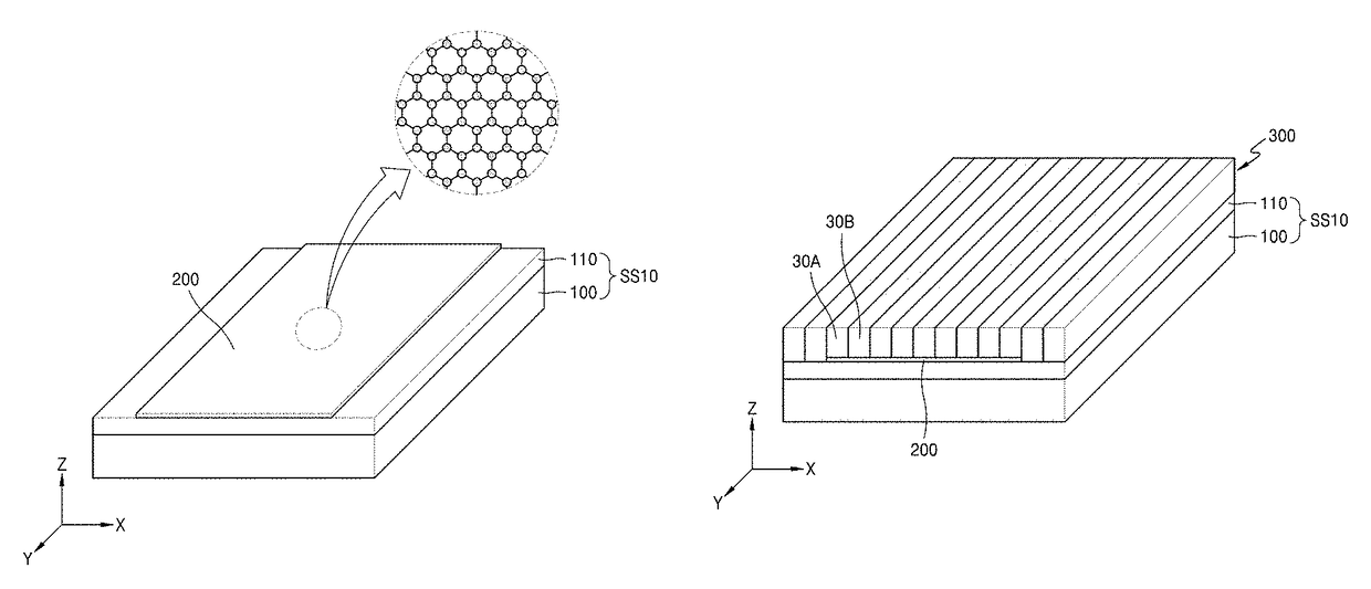
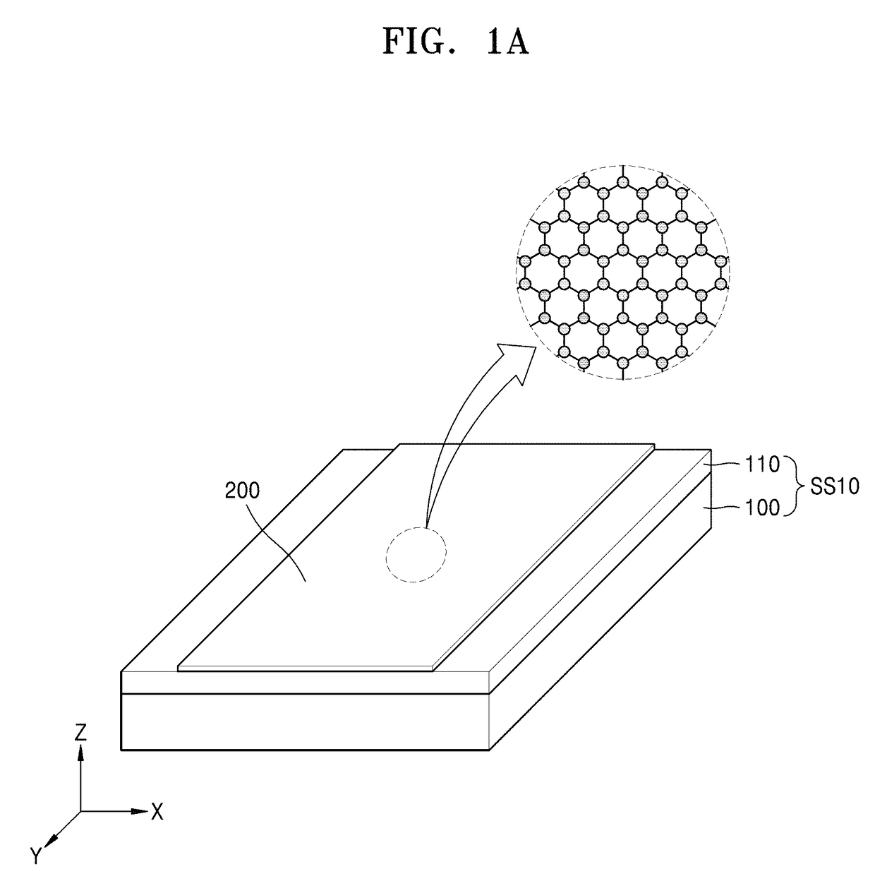
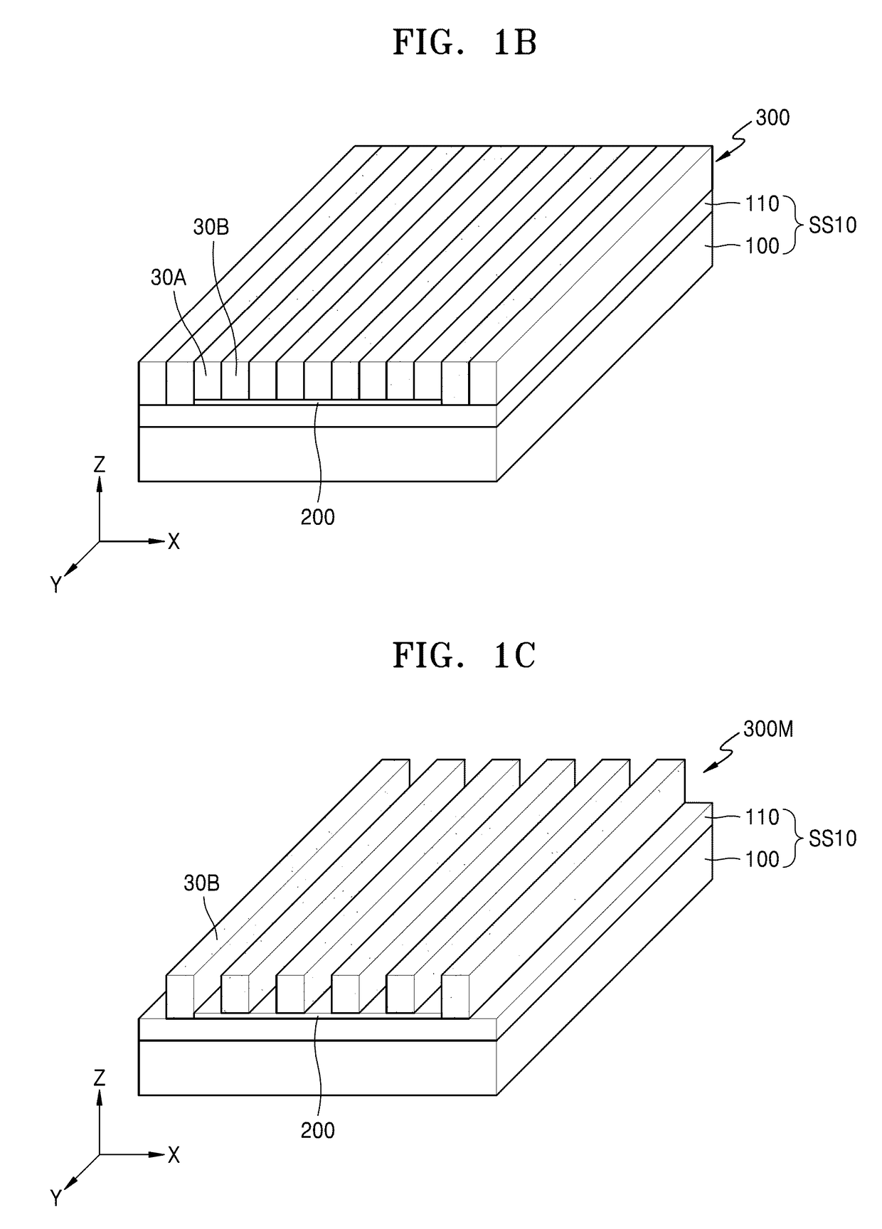
Methods of forming a graphene nanopattern, graphene-containing devices, and methods of manufacturing the graphene-containing devices are provided. A method of forming the graphene nanopattern may include forming a graphene layer on a substrate, forming a block copolymer layer on the graphene layer and a region of the substrate exposed on at least one side of the graphene layer, forming a mask pattern from the block copolymer layer by removing one of a plurality of first region and a plurality of second regions of the block copolymer, and patterning the graphene layer in a nanoscale by using the mask pattern as an etching mask. The block copolymer layer may be formed to directly contact the graphene layer. The block copolymer layer may be formed to directly contact a region of the substrate structure that is exposed on at least one side of the graphene layer.

Description

CROSS-REFERENCE TO RELATED APPLICATION[0001]This application claims priority under 35 U.S.C. §119 to Korean Patent Application No. 10-2015-0096788, filed on Jul. 7, 2015, in the Korean Intellectual Property Office, the disclosure of which is incorporated herein in its entirety by reference.BACKGROUND[0002]1. Field[0003]The present disclosure relates to methods of forming a graphene nanopattern, graphene-containing devices, and methods of manufacturing the graphene-containing devices.[0004]2. Description of Related Art[0005]Graphene, which is a hexagonal single layer structure composed of carbon atoms, may be structurally and chemically stable and may have exhibit excellent electrical and physical characteristics. For example, graphene may have a charge mobility (e.g., ˜2×105 cm2 / Vs) that is about 100 times or more faster than a charge mobility of silicon (Si), and may have a current density (e.g., about 108 A / cm2) that is about 100 times or more higher than a current density of copp...

Claims


Application Information

Patent Timeline
Patent Type & Authority Patents(United States)
IPC IPC(8): H01L21/308H01L29/66H01L29/778H01L51/00H01L21/467H01L29/06H01L21/3065H01L29/16B82Y10/00B82Y40/00H01L29/775
CPCH01L29/0676H01L21/3088H01L21/3065H01L21/3081H01L21/3085H01L29/1606H01L29/66037H01L29/66045H01L29/778H01L51/0045H01L21/3086H01L21/467H01L29/0673B82Y10/00B82Y40/00H01L29/775Y10S977/888H01L21/02527Y10S977/755H10K85/20H01L21/02603H01L21/042H01L21/823412H01L27/088H01L29/0665H01L29/78696
Inventor JEONG, SEONGJUNPARK, SEONGJUNLEE, YUNSEONG
Owner SAMSUNG ELECTRONICS CO LTD
Learn More