
Display device

a display device and thin technology, applied in static indicating devices, instruments, sport apparatuses, etc., can solve the problems of inability to allow an alloy mainly containing aluminum to have such a high potential, inherently not so resistant to pure aluminum, and significant galvanic corrosion caused by local cell phenomenon, etc., to achieve reliably high-quality display devices, easy and precise patterning

Active Publication Date: 2005-10-13
KOBE STEEL LTD
View PDF7 Cites 35 Cited by
  • Summary
  • Abstract
  • Description
  • Claims
  • Application Information

AI Technical Summary

Benefits of technology

The present invention provides a technique for easily and precisely patterning an aluminum alloy film for use in thin display devices and optical parts. The aluminum alloy film is a multilayer aluminum alloy film including a first aluminum alloy layer containing an aluminum alloy being substantially free from nitrogen, and a second aluminum alloy layer being adjacent to the first layer and including a nitrogen-containing aluminum alloy. The second aluminum alloy layer has been removed at least in a region where the pixel electrode is in contact with the multilayer aluminum alloy film, so as to allow the pixel electrode to be directly connected to the first aluminum alloy layer. The aluminum alloy film mainly contains aluminum and may further contain one or more alloy components. The thickness of the second aluminum alloy layer is preferably from about 5 to about 200 nm. The present invention provides a display device with high chemical resistance against, for example, alkaline developers and / or stripping solutions. The method for fabricating the display device is industrially advantageous.

Problems solved by technology

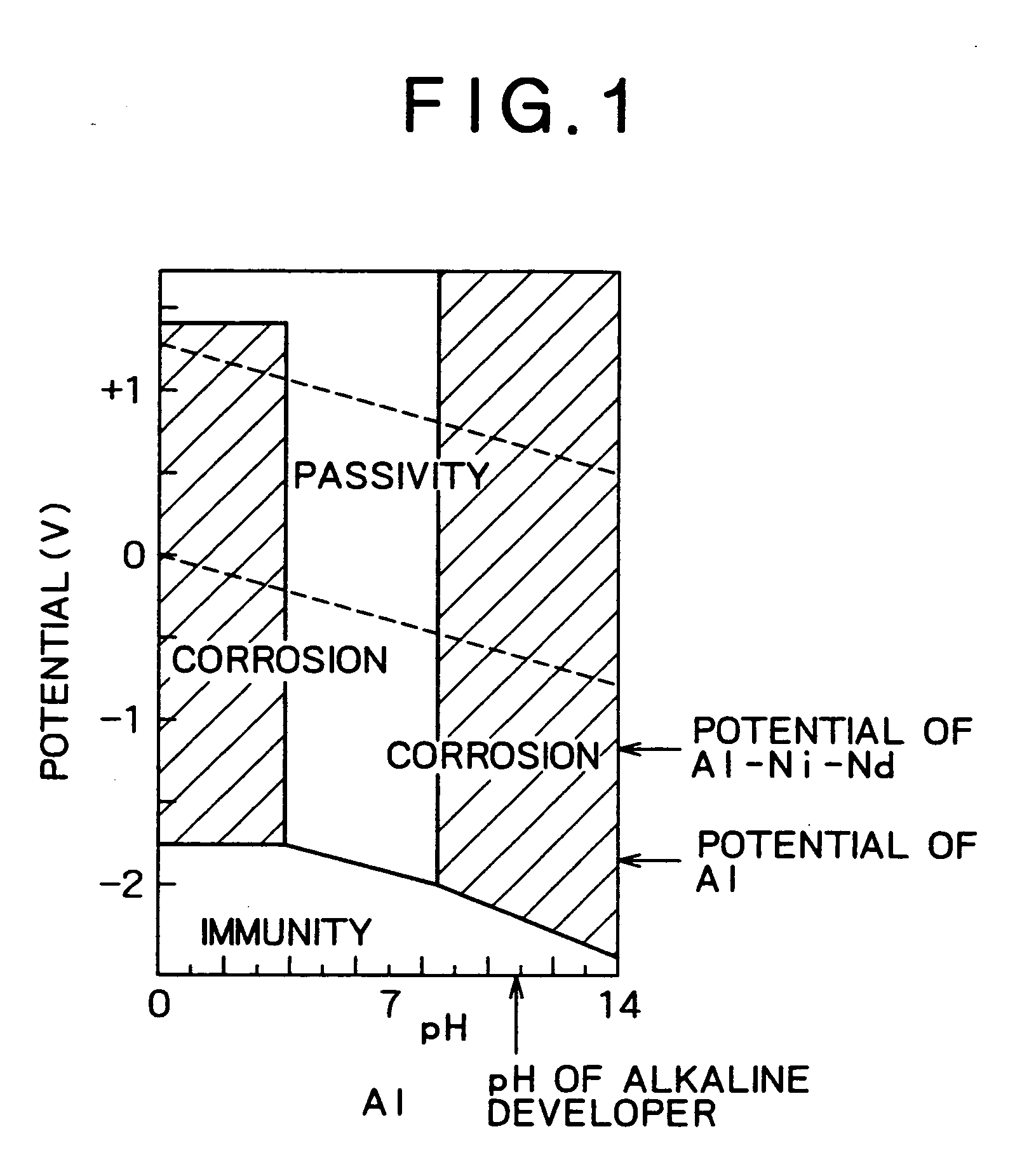
Aluminum is an amphoteric metal, and pure aluminum is inherently not so resistant against an acid and a base.
Galvanic corrosion caused by a local cell phenomenon becomes significant in such an alloy.
It is difficult, however, to allow an alloy mainly containing aluminum to have such a high potential, since the aluminum alloy must keep a low electric resistivity.
In other words, an aluminum alloy film in the wiring unit to be directly connected to the pixel electrode becomes more susceptible to corrosion than pure aluminum in terms of designing.
Organic aqueous alkaline developers, however, cannot be incorporated with an inhibitor and may invite corrosion.
In addition, a stripping agent containing an amine or its derivative for use in removal of a photoresist becomes alkaline when mixed with water.
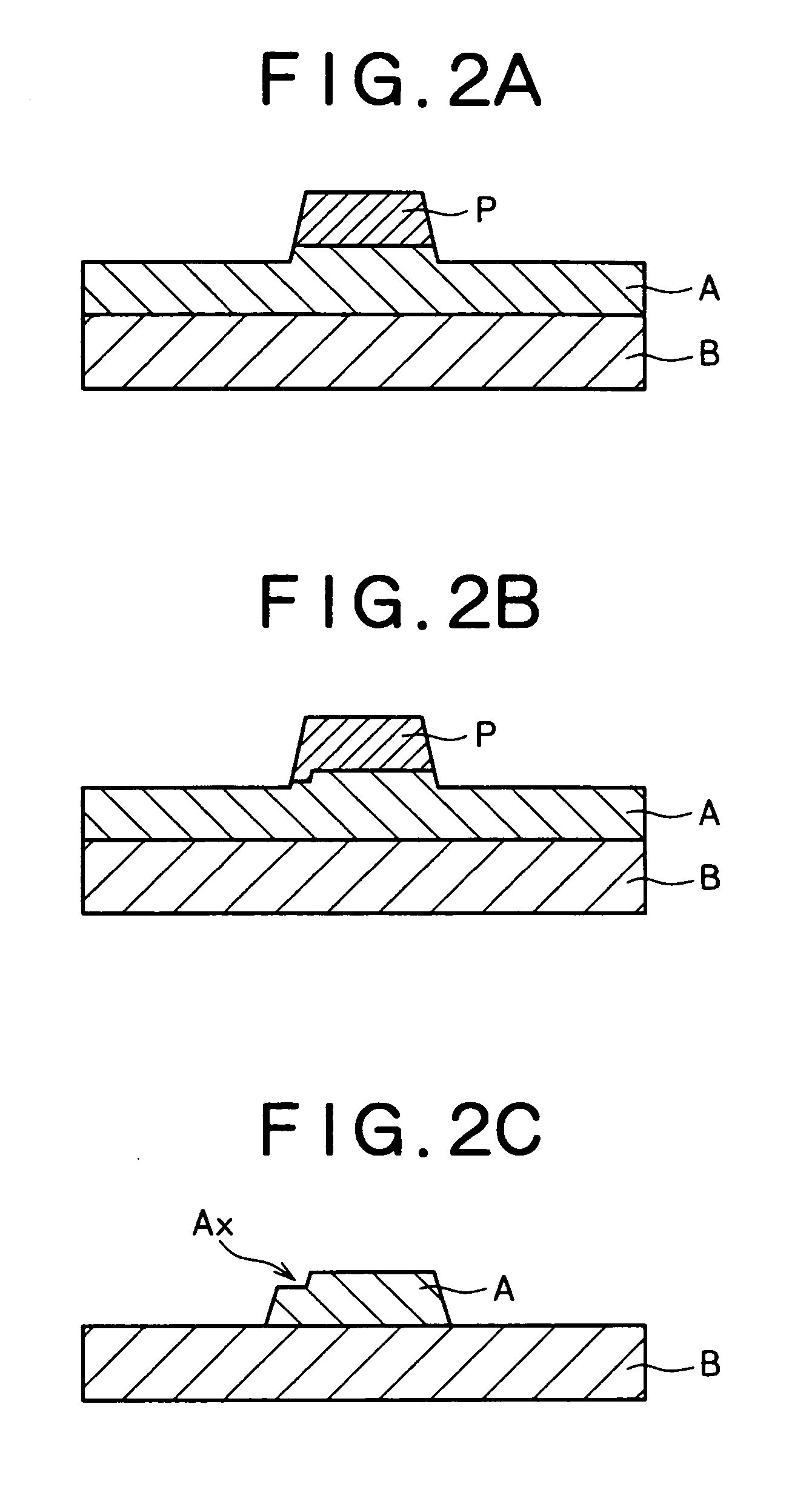
Misregistration of patterns formed by using a photoresist, however, may often occur in the photolithography process.
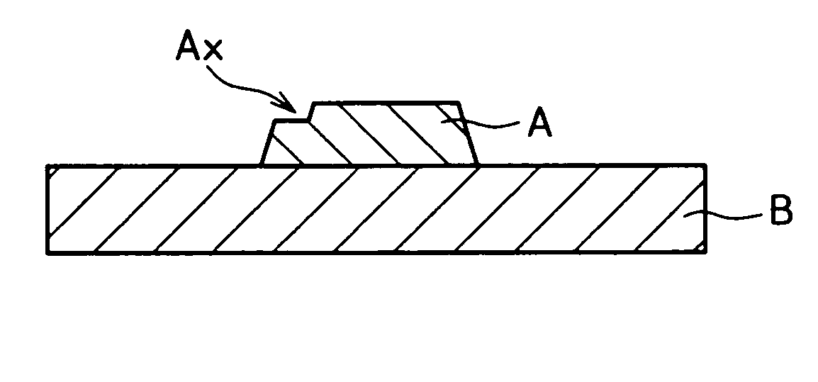
However, a pattern failure in which the aluminum alloy A is not covered by the photoresist, if occurred in the patterning process, invites misregistration in the rework process where the pattern is again covered by the photoresist (FIG. 2B), and the resulting step Ax remains to the last (FIG. 2C), which may invite contact failure.

Method used


Image

  • Display device
  • Display device
  • Display device

Examples


examples

[0116] The present invention will be illustrated in further detail with reference to several examples below, which are not intended to limit the scope of the present invention.

[0117] The contact resistance in direct contact between aluminum alloy wirings and the pixel electrode 5 on the array substrate according to the present invention was determined. The results are shown in Table 1.

[0118] The determination was carried out in the following manner.

[0119] 1) Configuration of the pixel electrode: Indium tin oxide (ITO) comprising indium oxide and 10 percent by weight of tin oxide and having a thickness of 200 nm, or indium zinc oxide (IZO) comprising indium oxide and 10 percent by weight of zinc oxide and having a thickness of 200 nm

[0120] 2) Configuration of the aluminum alloy film: The contents of the alloy components are shown in Table 1.

[0121] 3) Conditions for heat treatment: A dielectric film (SiNx) was formed to a thickness of 300 nm, and the work was subjected to heat tr...

examples 1 and 2

[0126] A silicon wafer bearing an oxide film (SiO2 thermally grown oxide film) 400 nm on its surface for establishing insulation of the substrate was used instead of the glass substrate. A nitrogen-free aluminum alloy film 300 nm thick was formed on the silicon wafer, a nitrogen-containing aluminum alloy film 30 nm thick was formed thereon to form a multilayer aluminum alloy film, the multilayer aluminum alloy film was patterned, and a dielectric film (SiNx) 300 nm thick was formed by chemical vapor deposition (CVD). The work was as intact subjected to heat treatment in a vacuum film-forming chamber for one hour and was taken out. A 80-μm square contact hole was patterned by photolithography, followed by etching with fluorine-containing plasma to thereby form a contact hole. In this procedure, overetching about 100% in terms of time was carried out in addition to the etching of the dielectric film. This treatment removed about 35 nm thick (about 11% of the film thickness) of the sur...

example 1

yer film comprising a nitrogen-containing Al-2 at % Ni-0.6 at % Nd and a nitrogen-free Al-2 at % Ni-0.6 at % Nd


PUM

PropertyMeasurementUnit
thicknessaaaaaaaaaa
standard electric potentialaaaaaaaaaa

Abstract

A display device includes an insulating substrate, a thin-film transistor arranged on the insulating substrate, a pixel electrode including a transparent electrode, and an aluminum alloy film as a connection wiring section for electrically connecting between the thin-film transistor and the pixel electrode. The aluminum alloy film is a multilayer aluminum alloy film including an aluminum alloy layer containing no nitrogen, and another aluminum alloy layer being arranged on the first layer and containing nitrogen. The nitrogen-containing layer ensures corrosion resistance against an alkaline solution. The nitrogen-containing aluminum alloy layer has been removed at least in a connection area with the pixel electrode so as to allow the pixel electrode to be directly connected to the first aluminum alloy layer.

Description

BACKGROUND OF THE INVENTION [0001] 1. Field of the Invention [0002] The present invention relates to a thin display device for use typically in semiconductors, liquid crystal displays and optical parts, and a method for fabricating the display device. [0003] 2. Description of the Related Art [0004] An active-matrix liquid crystal display device includes a thin-film transistor (TFT) array substrate, a counter substrate facing the TFT array substrate at a predetermined distance, and a liquid crystal layer sandwiched between the TFT array substrate and the counter substrate. The TFT array substrate includes TFTs as a switching element, pixel electrodes, and a wiring unit containing scanning lines and data lines. The counter substrate includes a common electrode. A passive-matrix liquid crystal display device includes a wiring substrate, a counter substrate facing the wiring substrate at a predetermined distance, and a liquid crystal layer arranged between the wiring substrate and the c...

Claims


Application Information

Patent Timeline
Patent Type & Authority Applications(United States)
IPC IPC(8): G02F1/1343G02F1/133G02F1/136G02F1/1362G02F1/1368H01L21/027H01L21/3205H01L21/336H01L21/768H01L21/77H01L21/84H01L23/52H01L27/12H01L29/04H01L29/786
CPCG02F1/136227G02F1/1368G02F1/13629H01L27/12H01L27/124A63F3/00694A63F2003/00927A63H33/18A63H33/26
Inventor GOTOH, HIROSHIKUGIMIYA, TOSHIHIROTOMIHISA, KATSUFUMI
Owner KOBE STEEL LTD
Learn More