Check patentability & draft patents in minutes with Patsnap Eureka AI!

Method for performing selective etching of a semiconductor material in solution

a technology of selective etching and semiconductor material, which is applied in the direction of semiconductor devices, basic electric elements, electrical appliances, etc., can solve the problems of reducing the performance of devices, reducing the selectivity of semiconductor materials, and increasing surface roughness, etc., to achieve high selectivity

Active Publication Date: 2017-11-28
COMMISSARIAT A LENERGIE ATOMIQUE ET AUX ENERGIES ALTERNATIVES
View PDF5 Cites 0 Cited by
  • Summary
  • Abstract
  • Description
  • Claims
  • Application Information

AI Technical Summary

Benefits of technology

This method achieves high selectivity and maintains the crystalline layer's surface roughness, enabling precise etching of amorphous silicon without damaging the crystalline silicon, thus enhancing device performance by avoiding unnecessary polishing steps.

Problems solved by technology

However, not only does a selectivity of 5 remain insufficient, but in addition these etchings are also generally accompanied by an increase of the roughness of the surfaces.
These etching methods can present a better selectivity, but they result in impairment of the components, which reduces the performances of the devices and / or requires subsequent polishing steps.

Method used


Image

  • Method for performing selective etching of a semiconductor material in solution
  • Method for performing selective etching of a semiconductor material in solution
  • Method for performing selective etching of a semiconductor material in solution

Examples


Embodiment Construction

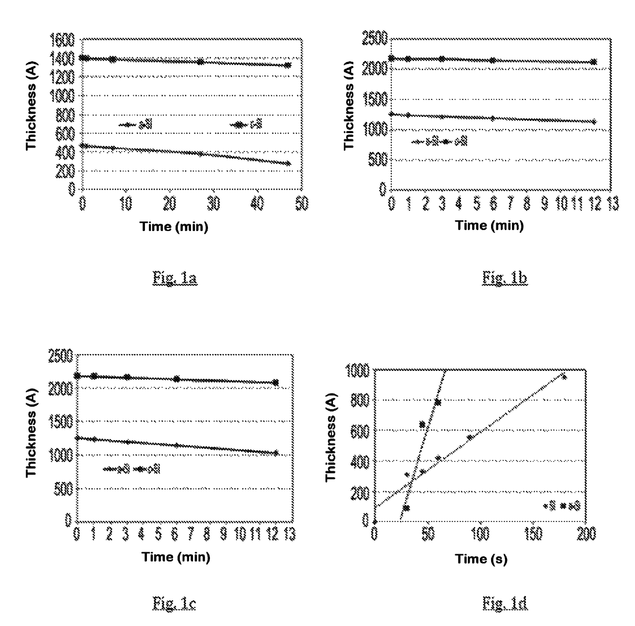
[0022]The method for performing selective etching of a layer of amorphous semiconductor material with respect to a layer of crystalline semiconductor material is an etching method in solution. What is meant hereinafter by crystalline is monocrystalline or polycrystalline.

[0023]What is meant by selective etching of a layer of amorphous semiconductor material with respect to a layer of crystalline semiconductor material is that, on completion of the etching step, the layer of crystalline semiconductor material is not etched, whereas the layer of amorphous semiconductor material is completely etched.

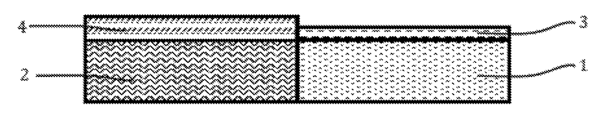
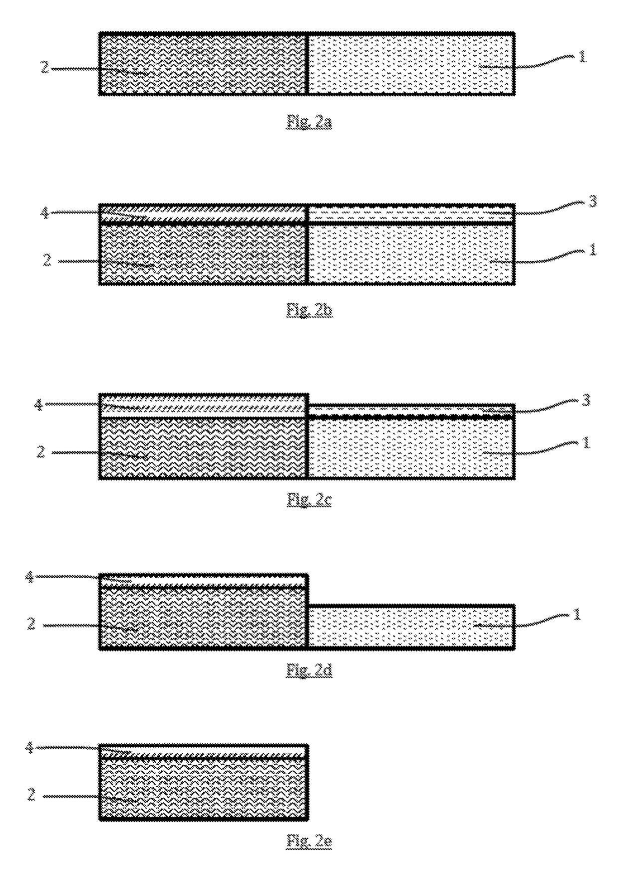
[0024]The method comprises the following successive steps (FIGS. 2a to 2e):[0025]a) providing a substrate comprising a layer of amorphous semiconductor material 1 to be etched and a layer of crystalline semiconductor material 2 (FIG. 2a),[0026]b) oxidising the surfaces of the layers of amorphous semiconductor material 1 and of crystalline semiconductor material 2 (FIG. 2b) so as to form a f...


PUM

PropertyMeasurementUnit
temperatureaaaaaaaaaa

Abstract

A method for performing selective etching of a semiconductor material in solution having the following successive steps: a) providing a substrate having a layer of amorphous semiconductor material to be etched and a layer of crystalline semiconductor material; b) oxidizing the surfaces of the layers of amorphous semiconductor material and of crystalline semiconductor material so as to form a first protective layer at the surface of the amorphous semiconductor material and a second protective layer at the surface of the crystalline semiconductor material; c) etching the first protective layer and the layer of amorphous semiconductor material with an alkaline etching solution, the etch rate v1 of the first protective layer being higher than the etch rate v2 of the second protective layer.

Description

BACKGROUND OF THE INVENTION[0001]The invention relates to a method for performing selective etching of a semiconductor material in solution.STATE OF THE ART[0002]An increasingly large number of methods for fabricating semiconductor-based electronic devices involve steps in which amorphous silicon has to be selectively etched on a substrate which comprises both amorphous silicon and crystalline silicon.[0003]Certain chemical solutions are known to enable selective etching of the layers of amorphous silicon with selectivity factors comprised between 2 and 5, i.e. the etching kinetics of the amorphous silicon are a maximum of 5 times faster than what can be obtained on crystalline silicon (FIGS. 1a to 1d). The etching solutions used are for example mixtures with a base formed by: water, ammonia, hydrogen peroxide, (FIG. 1a); acetic acid, hydrofluoric acid, hydrogen peroxide (FIG. 1b); water, sulphuric acid, hydrofluoric acid, hydrogen peroxide (FIG. 1c); tetramethylammonium hydroxide (...

Claims


Application Information

Patent Timeline
Patent Type & Authority Patents(United States)
IPC IPC(8): H01L21/311H01L29/04H01L21/02H01L21/306
CPCH01L21/30604H01L29/04H01L21/02236H01L21/02238H01L21/32105H01L21/32134H01L21/32139
Inventor LOUP, VIRGINIEBESSON, PASCAL
Owner COMMISSARIAT A LENERGIE ATOMIQUE ET AUX ENERGIES ALTERNATIVES
Features
  • R&D
  • Intellectual Property
  • Life Sciences
  • Materials
  • Tech Scout
  • Unparalleled Data Quality
  • Higher Quality Content
  • 60% Fewer Hallucinations
Learn More