Method of manufacturing resin multilayer substrate

a multi-layer substrate and manufacturing method technology, applied in the direction of multi-layer circuit manufacturing, printed circuits, electrical equipment, etc., can solve the problems of short-circuit defects or electric connection failures in vias, manufacturing methods that do not allow films (for example, pet films), and cannot provide carriers that function as masks, so as to reduce or prevent problems. , the effect of reducing or preventing

Active Publication Date: 2018-02-13
MURATA MFG CO LTD
View PDF19 Cites 0 Cited by
  • Summary
  • Abstract
  • Description
  • Claims
  • Application Information

AI Technical Summary

Benefits of technology

[0008]Preferred embodiments of the present invention provide methods of manufacturing a resin multilayer substrate that prevent undulation or the like of an insulation substrate during conveyance, and also significantly reduce or prevent spattering and falling off of a via-hole conductor.
[0014]According to various preferred embodiments of the present invention, in manufacturing a resin multilayer substrate, a cut for forming a cavity is made in the state where a carrier film is held in an insulation substrate (insulation sheet) before the subsequent conveyance is carried out. Accordingly, undulation or the like of the insulation substrate during conveyance thereof is significantly reduced or prevented. Therefore, it becomes possible to significantly reduce or prevent problems such as misalignment in stacking that occurs at the time when insulation substrates are stacked.
[0015]Furthermore, when a via-hole conductor is formed in an insulation substrate, a cut for forming a cavity is made in the state where a carrier film is held in the insulation substrate before paste for a via-hole conductor is charged. Accordingly, spattering and falling off of the paste for via-hole conductor are significantly reduced or prevented. Consequently, it becomes possible to significantly reduce or prevent the occurrence of short defects in a resin multilayer substrate and the occurrence of electric connection failures in a via-hole conductor.

Problems solved by technology

Accordingly, due to vibration caused by cutting and conveyance, the via conductor tends to spatter or fall off, which leads to short-circuit defects or electric connection failures in a via.
It is to be noted that this manufacturing method does not allow a film (for example, a PET film) functioning as a mask for via filling to be conveyed in the state where this film is held as a carrier film.
However, Japanese Patent Laying-Open No. 2005-322838 does not describe a manufacturing method of performing via filling, and also does not provide a carrier film functioning as a mask for via filling.

Method used


Image

  • Method of manufacturing resin multilayer substrate
  • Method of manufacturing resin multilayer substrate
  • Method of manufacturing resin multilayer substrate

Examples


first preferred embodiment

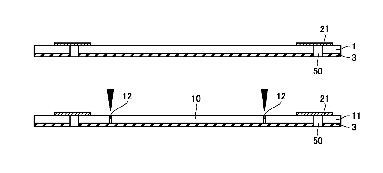
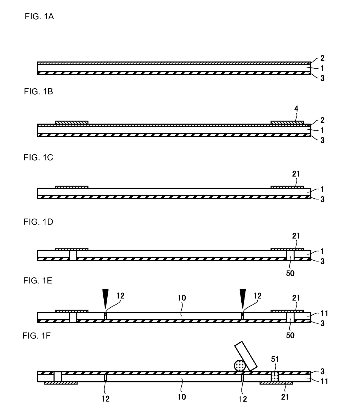
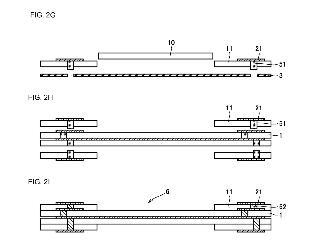
[0028]An example of the present invention will be described with reference to FIGS. 1A-1F and 2G-2I.

[0029]First, as shown in FIG. 1A, a conductor layer 2 is formed on one surface of an insulation substrate (insulation sheet) 1, and a carrier film 3 is affixed to the other surface thereof such that it can be peeled off. It is preferable that the carrier film has a certain retaining ability but also has slight adhesiveness by which excessive force is not required when this carrier film is peeled off.

[0030]Insulation substrate 1 includes a thermoplastic resin. The thermoplastic resin may be polyimide, a liquid crystal polymer (LCP), polyether ketone resin (PEEK), and polyphenylene sulfide resin (PPS), for example. In the case where the insulation substrate includes a thermoplastic resin, it is desirable that a heat treatment during pressing (collective thermocompression bonding) or the like after stacking is carried out at a relatively low temperature since resin tends to readily flow ...

second preferred embodiment

[0055]According to the present preferred embodiment, a portion of the insulation substrate that is cut out by a cut (unnecessary portion 10) has a shape (a cavity portion) including at least one corner portion that has a circumference portion having a prescribed radius of curvature R (FIG. 6B). In FIG. 6B, the corners of the shape as shown in FIG. 6A are rounded such that the corners are eliminated. The present preferred embodiment is different in this feature from the first preferred embodiment, but preferably identical in other features to the first preferred embodiment. It is to be noted that the shape described herein means the shape as viewed from the normal direction of the main surface of the insulation substrate.

[0056]In addition, as to insulation substrate 11 including unnecessary portion 10 having the shape as described above, a plurality of insulation substrates 11 are simultaneously fabricated from substrate base material 100, as shown in FIG. 7.

[0057]When at least one o...


PUM

PropertyMeasurementUnit
thicknessaaaaaaaaaa
surface roughnessaaaaaaaaaa
thicknessaaaaaaaaaa

Abstract

A method of manufacturing a resin multilayer substrate with a cavity, includes stacking insulation substrates including thermoplastic resins and thermocompression-bonding the insulation substrates. At least one of the insulation substrates is formed by affixing a peelable carrier film to one main surface of the insulation substrate, making a cut in the insulation substrate having the carrier film affixed thereto, the cut being designed to form the cavity, penetrating the insulation substrate in a thickness direction and not penetrating the carrier film in a thickness direction, and removing the carrier film and a portion of the insulation substrate that is cut out by the cut.

Description

BACKGROUND OF THE INVENTION[0001]1. Field of the Invention[0002]The present invention relates to a method of manufacturing a resin multilayer substrate.[0003]2. Description of the Related Art[0004]A resin multilayer substrate having a rigid portion and a flexible portion is known. Such a resin multilayer substrate consists of a flexible portion (a portion that is thinner or has fewer layers and higher flexibility) and a rigid portion (a portion that is thicker or has more layers and lower flexibility). The rigid portion is different from the flexible portion in a number of insulation substrates or in a composition material of the insulation substrate. Furthermore, as a method of manufacturing a resin multilayer substrate, there is a known method by which resin sheets, each made of a thermoplastic resin and having a conductor pattern formed thereon are stacked, then heated and pressurized by a heat pressing plate, and collectively bonded as a stacked body.[0005]Japanese Patent Laying...

Claims


Application Information

Patent Timeline
Patent Type & Authority Patents(United States)
IPC IPC(8): H05K3/46H05K3/00H05K3/40
CPCH05K3/4632H05K3/005H05K3/4691H05K3/4053Y10T29/49165H05K2203/0228Y10T29/49124Y10T29/49126Y10T29/49162H05K2203/0191
Inventor KOTSUBO, TAKUYACHISAKA, SHUNSUKE
Owner MURATA MFG CO LTD
Why Eureka
Try Eureka