Method of manufacturing resin multilayer substrate
- Summary
- Abstract
- Description
- Claims
- Application Information
AI Technical Summary
Benefits of technology
Problems solved by technology
Method used
Image
Examples
first preferred embodiment
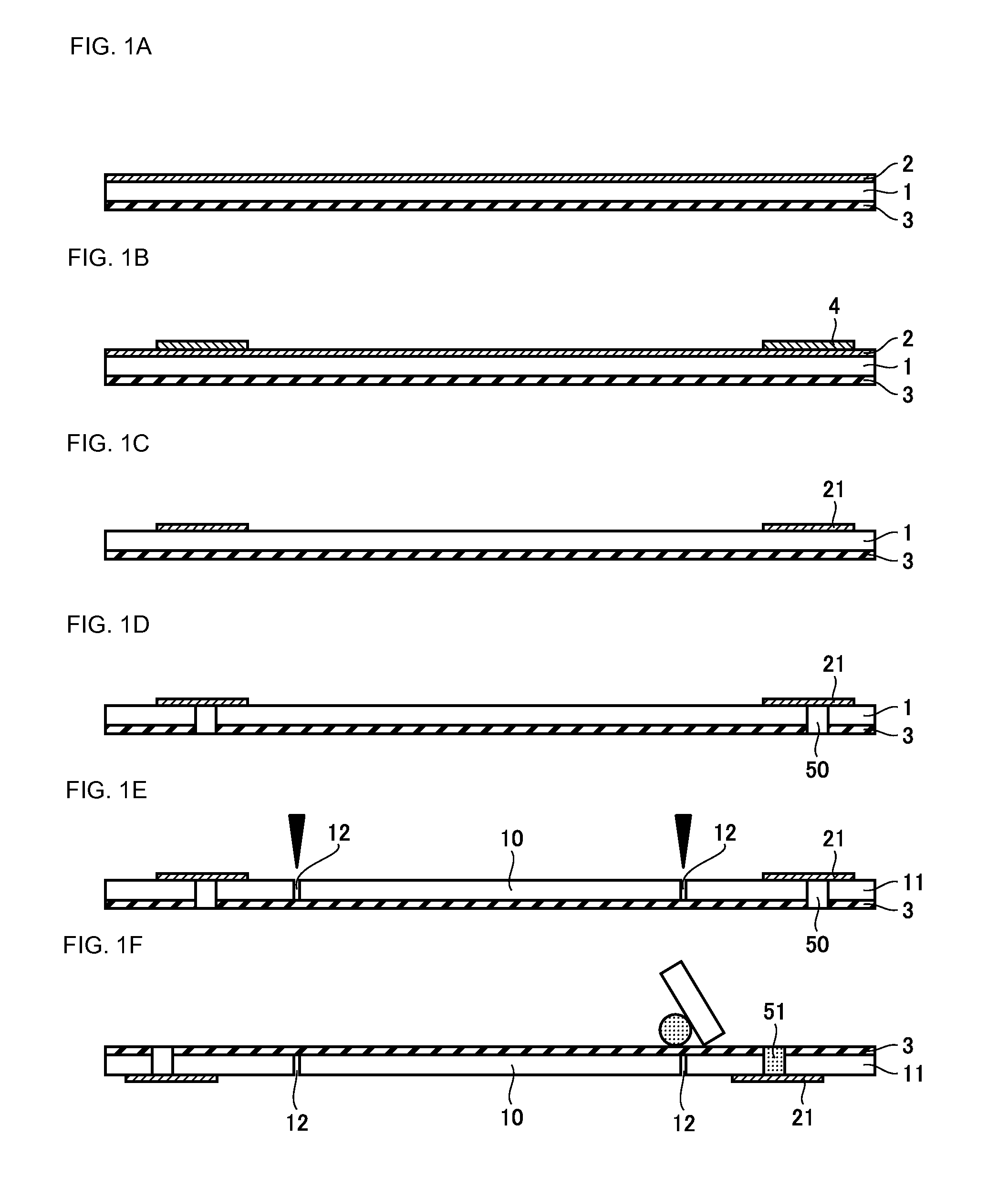
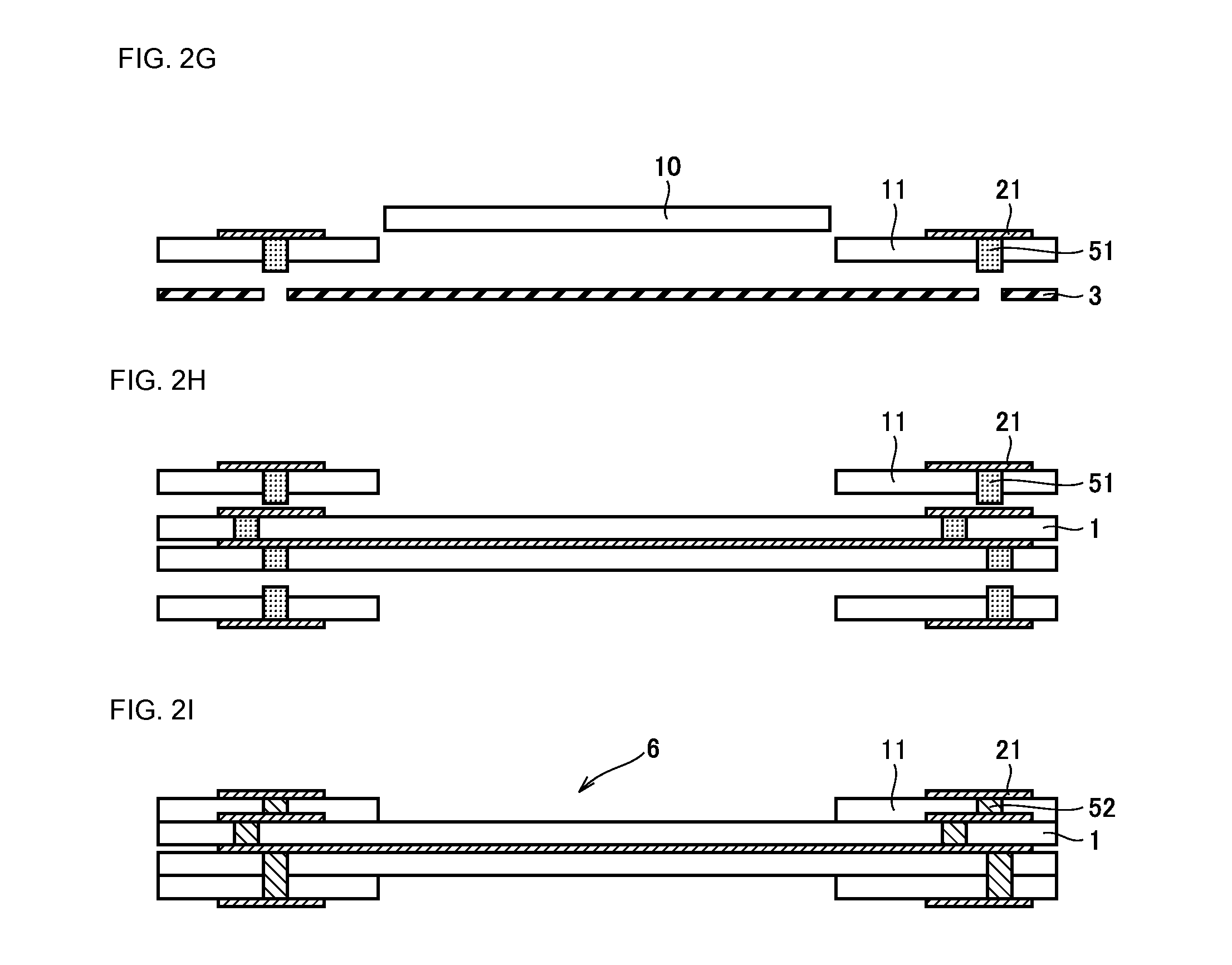
[0028]An example of the present invention will be described with reference to FIGS. 1A-1F and 2G-2I.
[0029]First, as shown in FIG. 1A, a conductor layer 2 is formed on one surface of an insulation substrate (insulation sheet) 1, and a carrier film 3 is affixed to the other surface thereof such that it can be peeled off. It is preferable that the carrier film has a certain retaining ability but also has slight adhesiveness by which excessive force is not required when this carrier film is peeled off.
[0030]Insulation substrate 1 includes a thermoplastic resin. The thermoplastic resin may be polyimide, a liquid crystal polymer (LCP), polyether ketone resin (PEEK), and polyphenylene sulfide resin (PPS), for example. In the case where the insulation substrate includes a thermoplastic resin, it is desirable that a heat treatment during pressing (collective thermocompression bonding) or the like after stacking is carried out at a relatively low temperature since resin tends to readily flow ...
second preferred embodiment
[0055]According to the present preferred embodiment, a portion of the insulation substrate that is cut out by a cut (unnecessary portion 10) has a shape (a cavity portion) including at least one corner portion that has a circumference portion having a prescribed radius of curvature R (FIG. 6B). In FIG. 6B, the corners of the shape as shown in FIG. 6A are rounded such that the corners are eliminated. The present preferred embodiment is different in this feature from the first preferred embodiment, but preferably identical in other features to the first preferred embodiment. It is to be noted that the shape described herein means the shape as viewed from the normal direction of the main surface of the insulation substrate.
[0056]In addition, as to insulation substrate 11 including unnecessary portion 10 having the shape as described above, a plurality of insulation substrates 11 are simultaneously fabricated from substrate base material 100, as shown in FIG. 7.
[0057]When at least one o...
PUM
| Property | Measurement | Unit |
|---|---|---|
| Thickness | aaaaa | aaaaa |
| Radius | aaaaa | aaaaa |
| Electrical conductor | aaaaa | aaaaa |
Abstract
Description
Claims
Application Information


