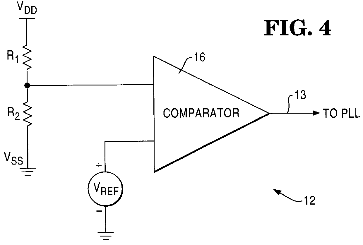
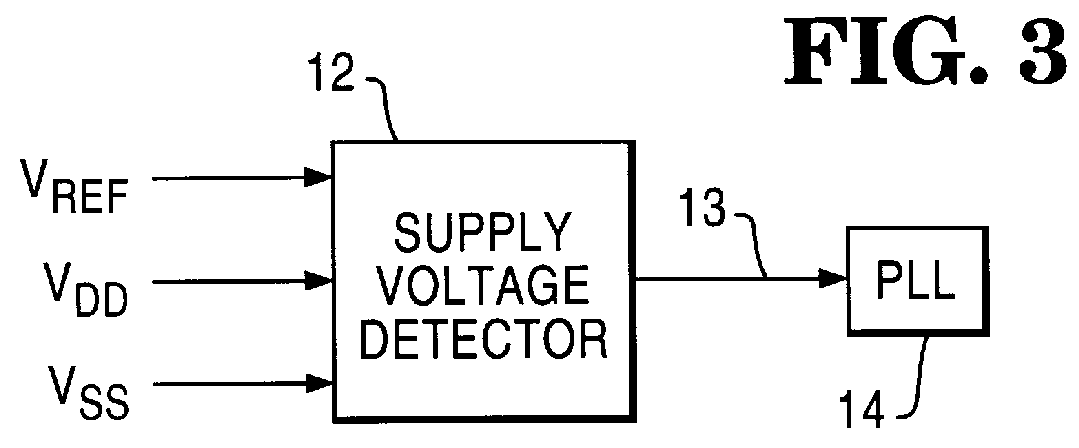
FIG. 3 shows how to adjust the frequency range of a PLL based on supply voltage. First, the power supply voltage level is detected by detector 12. The detector output 13 is coupled to the PLL 14. Supply voltage detector 12 operates by comparing the supply voltage VDD with a reference voltage VREF which is independent of the supply voltage. The reference voltage VREF can come from an external voltage regulator or be generated on-chip by a bandgap reference voltage source. Since the reference voltage VREF will generally be lower than the supply voltage VDD, the reference voltage cannot be compared directly with the supply voltage. Rather, the supply voltage is scaled and compared with the reference voltage. There are many possible ways to scale down the supply voltage. One way is to use a voltage divider as shown in FIG. 4. If all that is needed is to operate the PLL at 3.3 V and 5 V, a divide-by-two voltage divider R1/R2 is used to scale the supply voltage VDD from 3.3 V to 1.65 V and from 5 V to 2.5 V. For an equal margin on both sides, a 2.075 V reference voltage VREF is used to detect the supply voltage.
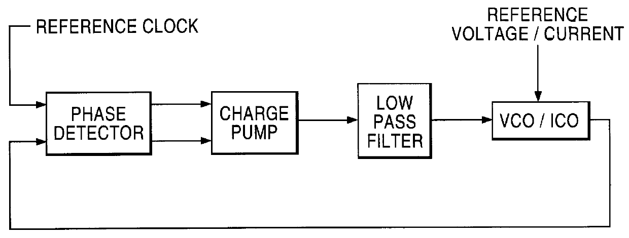
Once the supply voltage level is detected, the next step is to find a way to adjust the PLL frequency range accordingly. A possible solution is to insert a frequency divider which can be enabled when operated at 5 V to divide down the PLL output frequency. FIG. 5 shows a phase-locked loop 14 comprising a phase detector 18, charge pump 20, low pass filter 22 and VCO/ICO 24. However, as also shown in FIG. 5, the PLL has been modified to include a frequency divider 26 between the VCO/ICO 24 and the phase detector 18. The output 27 from the frequency divider 26 is selected by the multiplexer 28 if a 5 V supply voltage is detected, as indicated by control line 13 (which may be generated by the circuit shown in FIG. 4).
However, there are a few drawbacks associated with this approach. First of all, the frequency divider 26 requires extra silicon area and consumes extra power at relatively high frequency. Secondly, if a non-integer divider is required, it could be difficult to implement. An easier way to adjust the PLL frequency range is to adjust the reference voltage or current 40 that goes into the PLL. Most of the VCO (Voltage-Controlled Oscillator) or ICO (Current-Controlled Oscillator) based PLLs have either an external voltage or current source that determines the PLL's center operating frequency, one such oscillator being described in U.S. Pat. No. 5,302,920 entitled "Controllable Multi-Phase Ring Oscillators with Variable Current Sources and Capacitances", which is hereby incorporated by reference. By changing the reference voltage or current 40, the PLL frequency range can be adjusted based on the detected supply voltage.
FIG. 6 gives an example on how this can be done by adding two transistors M1 and M2, which function as a voltage to current (V-I) converter 34. The reference current going into the PLL at 40, which is the sum of current source output 36 and V-I converter output 38, is reduced by turning off the transistor M1 when a 5V power supply voltage is detected, as indicated by control line 13. If a 3.3 V power supply voltage is detected, transistor M1 is turned on, and supplies additional current to the PLL via output 38 to PLL input 40.
FIG. 7 shows how to operate the PLL at both 3.3 V and 5 V. It is even better if the frequency range could be adjusted linearly with the supply voltage so that the PLL could operate at any supply voltage level. This is done by replacing the comparator 16 of FIG. 4 with a differential amplifier, as shown at 30 in FIG. 8. The output 52 of the differential amplifier is proportional to the difference between the supply-independent reference voltage VREF and the scaled supply voltage VDD. This output voltage 52 is then used to adjust the reference voltage/current going into the PLL, similar to the technique that was previously described with respect to FIG. 6. However, since the differential amplifier provides an analog output voltage (as opposed to a digital output from the comparator of FIG. 7), a simplified voltage to current converter 44 is used.
As shown in FIG. 9, the simplified voltage to current converter only requires a single transistor M3, which is biased by the output voltage 52 from the differential amplifier 30.
The circuit of FIG. 8 thus provides a technique for adjusting the reference current linearly with the supply voltage, such that the PLL can operate at a plurality of dissimilar supply voltages.
While I have illustrated and described the preferred embodiments of our invention, it is to be understood that I do not limit myself to the precise constructions herein disclosed, and the right is reserved to all changes and modifications coming within the scope of the invention as defined in the appended claims.