Method for solidifying frame glue and meethod for making liquid crystal display panel by using sad method

A liquid crystal panel and frame glue technology, which is applied in the direction of identification devices, nonlinear optics, instruments, etc., can solve the problems of complex process, inability to use black matrix and color film, and inability to use ultraviolet curing process, so as to avoid UV absorption.

A liquid crystal panel and frame glue technology, which is applied in the direction of identification devices, nonlinear optics, instruments, etc., can solve the problems of complex process, inability to use black matrix and color film, and inability to use ultraviolet curing process, so as to avoid UV absorption.

CN100361011CInactive Publication Date: 2008-01-09AU OPTRONICS CORP

Image

  • Method for solidifying frame glue and meethod for making liquid crystal display panel by using sad method
  • Method for solidifying frame glue and meethod for making liquid crystal display panel by using sad method
  • Method for solidifying frame glue and meethod for making liquid crystal display panel by using sad method

Examples


Embodiment Construction

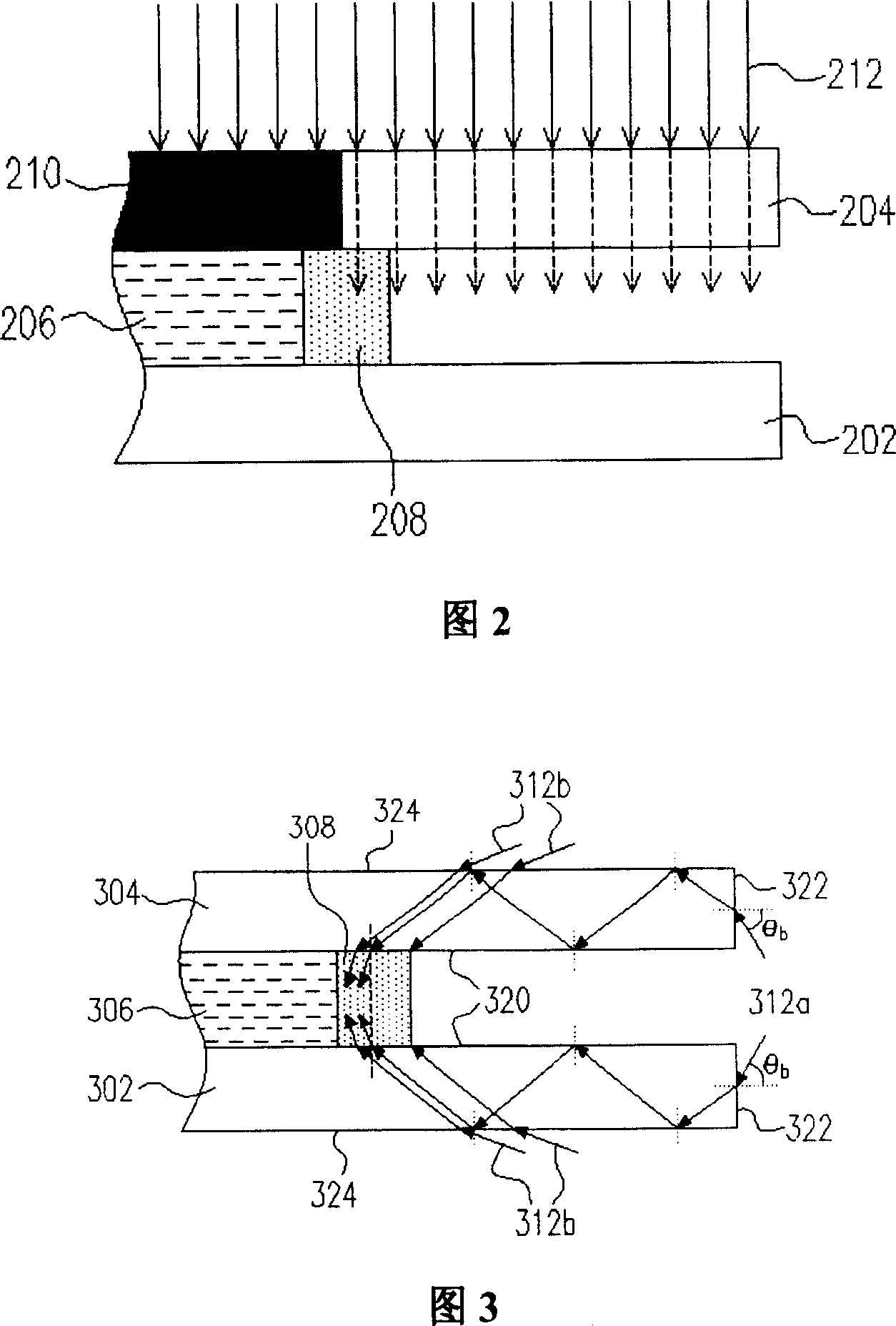
[0040]FIG. 3 is a schematic cross-sectional view of a liquid crystal panel according to a preferred embodiment of the present invention when curing a sealant process. Please refer to FIG. 3 , the method proposed by the present invention is suitable for curing a sealant 308 positioned between a first substrate 302 and a second substrate 304 , wherein the first substrate 302 and the second substrate 304 both include a front surface 320 , a back surface 324 and a side surface 322, and the front surface 320 of the first substrate 302 and the second substrate 304 are opposite. The material of the frame glue 308 is, for example, UV glue. The width of the frame glue 308 is, for example, between 1000-1200 microns, and the thickness is, for example, about 5 microns. The material of the first substrate 302 and the second substrate 304 is, for example, glass.

[0041] Please continue to refer to FIG. 3 , the curing method of this embodiment is to use the law of total internal reflection...


PUM

PropertyMeasurementUnit
widthaaaaaaaaaa
thicknessaaaaaaaaaa

Abstract

The invention provides a method of solidifying deckle glue and a method of making LCD panel by the solidifying method, where the former is adaptive to the deckle glue with the solidification site between the first and second basal plates, its character: using total reflection law, it makes a UV light incident into the two basal plates at a give angle, and makes the UV light enter into the deckle glue when the UV light meets with the deckle glue instead of the liquid crystal.

Description

technical field [0001] The present invention relates to a manufacturing method of a liquid crystal display (LCD for short), and particularly relates to a method of curing a sealant and a method of manufacturing a liquid crystal panel using the method. Background technique [0002] With the development of high technology, video products, especially digital video or image devices have become common products in daily life. In these digital video or image devices, the display is an important component to display relevant information. Users can read information from the display, or further control the operation of the device. [0003] In order to match the modern life style, the volume of video or image devices is becoming thinner and lighter. Although the traditional cathode-layer ray display still has its advantages, it needs to occupy a large volume and consumes power. Therefore, in combination with optoelectronic technology and semiconductor manufacturing technology, panel...

Claims


Application Information

Patent Timeline
09 Jan 2008
Publication
CN100361011C
IPC
G02F1/1341; G02F1/1339; G02F1/1333; G09F9/35
Inventors
εˆ˜εΎ—ε…‰; 吕仁贡