Semiconductor integrated circuit device
A technology of integrated circuits and semiconductors, which is applied in the field of semiconductor integrated circuit devices, and can solve problems such as the widening of the power supply unit 6a
- Summary
- Abstract
- Description
- Claims
- Application Information
AI Technical Summary
Problems solved by technology
Method used
Image

Examples
Embodiment approach 1
[0061] This embodiment will describe an example in which the power supply terminal of the internal circuit is set or arranged near the internal power supply wiring instead of close to the signal power supply terminal.
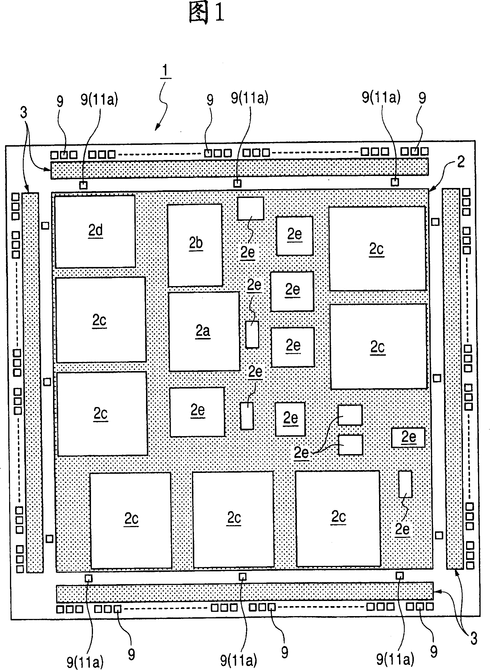
[0062] 1 is a typical plan view showing the layout of a microcomputer (semiconductor integrated circuit device) shown in Embodiment Mode 1;
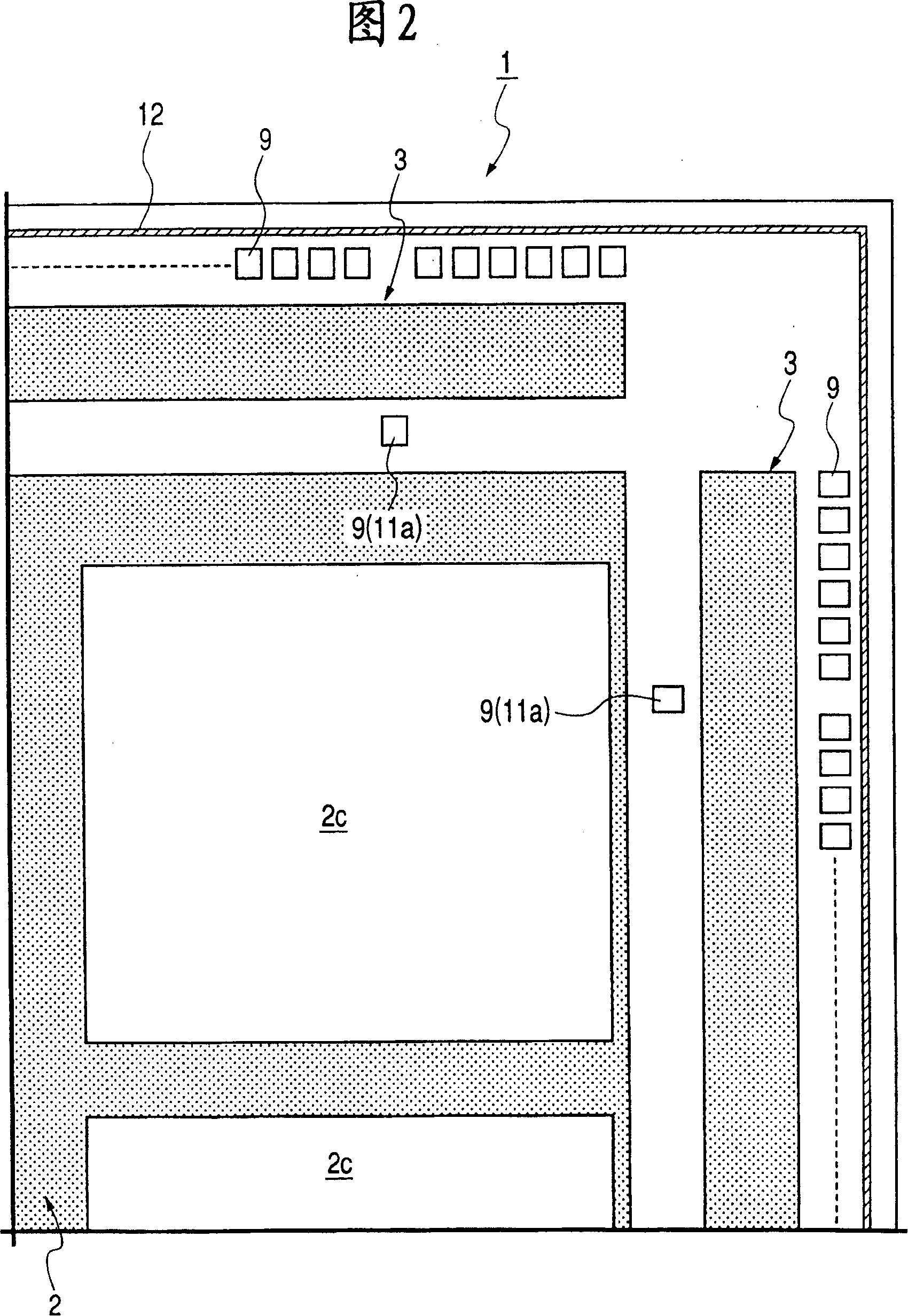
[0063] Figure 2 is an enlarged typical plan view of the part depicted in Figure 1;
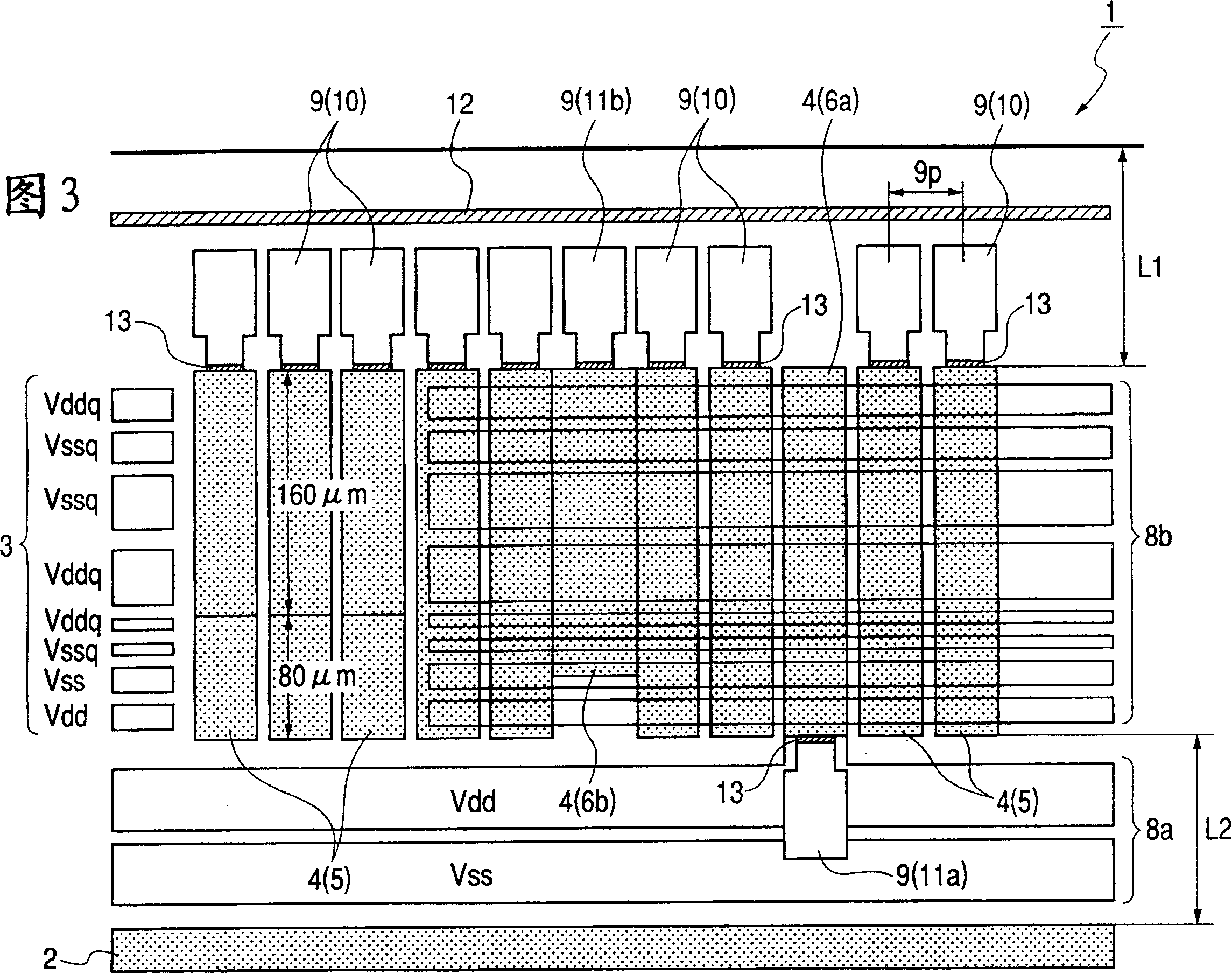
[0064] Figure 3 is an enlarged typical plan view of the portion illustrated in Figure 2;
[0065] Fig. 4 is a typical plan view partially enlarged as shown in Fig. 3;
[0066] Fig. 5 is a block diagram illustrating the schematic structure of the signal unit shown in Fig. 4;
[0067] Fig. 6 is a block diagram illustrating the schematic structure of the internal circuit power supply unit shown in Fig. 4;
[0068] Fig. 7 is an equivalent circuit diagram showing an example of an input / output circuit incorporated in the signal unit shown in...
Embodiment approach 2
[0103] The present invention will describe an example in which pads are provided on the input / output unit.
[0104] FIG. 13 is a typical plan view showing the layout of the microcomputer described in Embodiment 2, and FIG. 14 is a typical plan view showing a part shown in FIG. 13 enlarged.
[0105] As shown in FIGS. 13 and 14 , a plurality of bonding pads 9 are provided within the outer ends of their respective input / output units 4 . In this embodiment, a plurality of bonding pads 9 are arranged to overlap their corresponding input / output units in a planar manner. With such a structure, the distance L1 between the edge of the semiconductor chip 1 and the outer end of each input / output unit 4 can be shortened. Therefore, it is possible to downsize the semiconductor chip 1 (microcomputer).
[0106] In order to avoid the stress during press-fitting and the impact when making columnar bumps, any circuit whose characteristics and breakdown are in danger of degrading due to stress...
Embodiment approach 3
[0108] FIG. 15 is a typical plan view showing the layout of the microcomputer described in Embodiment 3, and FIG. 16 is a typical plan view showing a part of FIG. 15 enlarged.
[0109] As shown in FIGS. 15 and 16, internal circuit power supply terminals 11a are respectively provided inside the input / output unit 4 so as to overlap the internal circuit power supply wiring 8a in a planar manner. The signal terminal 10 and the power supply terminal 11b of the I / O unit are arranged to overlap their corresponding I / O unit 4 in a planar manner. Therefore, the width of each inner circuit power supply unit 6a can be narrowed. With such a structure, the size of the semiconductor chip 1 (microcomputer) can be made smaller.
PUM
 Abstract
Description
Claims
Application Information
 - R&D Engineer
- R&D Manager
- IP Professional
- Industry Leading Data Capabilities
- Powerful AI technology
- Patent DNA Extraction
Browse by: Latest US Patents, China's latest patents, Technical Efficacy Thesaurus, Application Domain, Technology Topic.
© 2024 PatSnap. All rights reserved.Legal|Privacy policy|Modern Slavery Act Transparency Statement|Sitemap