Liquid crystal display device

A technology of liquid crystal display device and liquid crystal layer, applied in optics, instruments, nonlinear optics, etc., can solve the problems of increased power consumption of display devices, decreased brightness and contrast of display devices, and increased power consumption of liquid crystal display devices, etc. The effect of low power consumption and good display quality

Inactive Publication Date: 2008-03-26
HONG FU JIN PRECISION IND (SHENZHEN) CO LTD +1
View PDF6 Cites 0 Cited by
  • Summary
  • Abstract
  • Description
  • Claims
  • Application Information

AI Technical Summary

Problems solved by technology

[0004] Since the IPS type liquid crystal display device 1 cannot utilize ambient light to provide illumination for the display, the display of the liquid crystal display device 1 needs to rely on the illumination emitted by its backlight module (not shown), because the backlight module is the entire liquid crystal display device. The main energy-consuming device of the LCD device accounts for about half of all energy consumption. If only relying on the backlight module to provide lighting and cannot use ambient light sources to provide lighting, the energy consumption of the entire LCD device will increase, which is not conducive to energy saving
Moreover, when the liquid crystal display device is placed in an environment with strong external light, the brightness and contrast of the liquid crystal display device will decrease, so the display quality of the liquid crystal display device is greatly affected by the external environment. In order to maintain the brightness of the liquid crystal display device If the degree and contrast ratio are high, the power of the backlight module must be increased, and the power consumption of the liquid crystal display device will also increase accordingly.

Method used


Image

  • Liquid crystal display device
  • Liquid crystal display device
  • Liquid crystal display device

Examples


Embodiment Construction

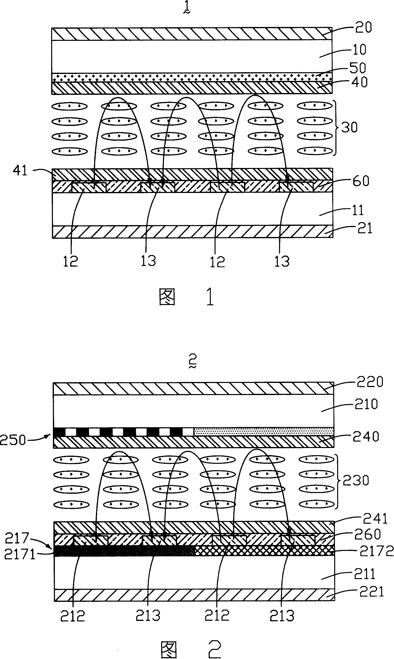
[0018] FIG. 2 is a schematic structural view of the first embodiment of the liquid crystal display device of the present invention. The liquid crystal display device 2 of the present invention includes an upper substrate 210 , a lower substrate 211 opposite to the upper substrate 210 , and a liquid crystal layer 230 sandwiched between the two substrates 210 , 211 . A color filter 250 and an upper alignment layer 240 are sequentially disposed on the inner surface of the upper substrate 210 , and an upper polarizer 220 is disposed outside the upper substrate 210 . The inner surface of the lower substrate 211 is provided with a common electrode 212, an insulating layer 260, a pixel electrode 213, a semi-reflective layer 217, and a lower alignment layer 241, wherein the common electrode 212 and the pixel electrode 213 are arranged in parallel and spaced apart, and can be straight Strip or curved strip structure. A lower polarizer 221 is disposed outside the lower substrate 211 . ...


PUM


Abstract

This invention relates to a LCD device including a top base board, a bottom base board, a pixel electrode, a common electrode, a LC layer and a color filter, among which, said pixel electrode and said common electrode are set on the bottom base board, the electric fields parallel to the bottom base board formed by the pixel and common electrodes have horizontal vectors, said LC layer is packed between the two base boards, said color filter is set between said LC layer and the top base board including a transparent base, a black matrix, a tinted layer and a transparent protection layer, said tinted layer includes a first part and a second part said first part corresponds to the pixel and common electrodes, a semi-reflection layer is set on the bottom base board, the first part of the tinted layer is set with multiple holes.

Description

【Technical field】 [0001] The invention relates to a liquid crystal display device, in particular to a liquid crystal display device using wide viewing angle technology. 【Background technique】 [0002] The liquid crystal itself in the liquid crystal display device does not have luminescent properties, it uses an electric field to control the twisting of the liquid crystal molecules to pass or not to pass light, so as to achieve the purpose of display. In a traditional liquid crystal display device, electrodes are formed on the surfaces of two glass substrates to form an electric field that controls the twisting of liquid crystal molecules. The electrodes use transparent materials, and the electrodes of the two substrates are oppositely arranged to form an electric field perpendicular to the surface of the substrates. . Because the liquid crystal molecules have electrical properties, under the control of the electric field, the orientation of the liquid crystal molecules will...

Claims


Application Information

Patent Timeline
Patent Type & Authority Patents(China)
IPC IPC(8): G02F1/1343G02F1/136G02B5/23
Inventor 杨秋莲陈鹊如
Owner HONG FU JIN PRECISION IND (SHENZHEN) CO LTD
Why Eureka
Try Eureka