Supercharge Your Innovation With Domain-Expert AI Agents!

Polishing device and substrate processing device

A polishing device and substrate processing technology, which can be used in grinding devices, transportation and packaging, electrical components, etc., and can solve problems such as decreased productivity, large moving space for handling robots, and delayed wafer handling.

Inactive Publication Date: 2008-04-09
EBARA CORP
View PDF6 Cites 0 Cited by
  • Summary
  • Abstract
  • Description
  • Claims
  • Application Information

AI Technical Summary

Problems solved by technology

[0005] However, in the above-mentioned polishing apparatus, since it is necessary to install a pusher on each polishing unit, the installation space of the pusher is large, and the movement of the transfer robot for transferring the wafer between these pushers is very large. The space is very large, and the device is large-scaled
In addition, since the above-mentioned transfer robot cannot transfer a plurality of wafers at a time, when the above-mentioned transfer robot is used in various applications, when the transfer robot is restricted in order to transfer other wafers, the transfer of the required wafer will be delayed.
In this case, wafer processing and transportation cannot be performed efficiently, resulting in a drop in productivity.

Method used


Image

  • Polishing device and substrate processing device
  • Polishing device and substrate processing device
  • Polishing device and substrate processing device

Examples


Embodiment Construction

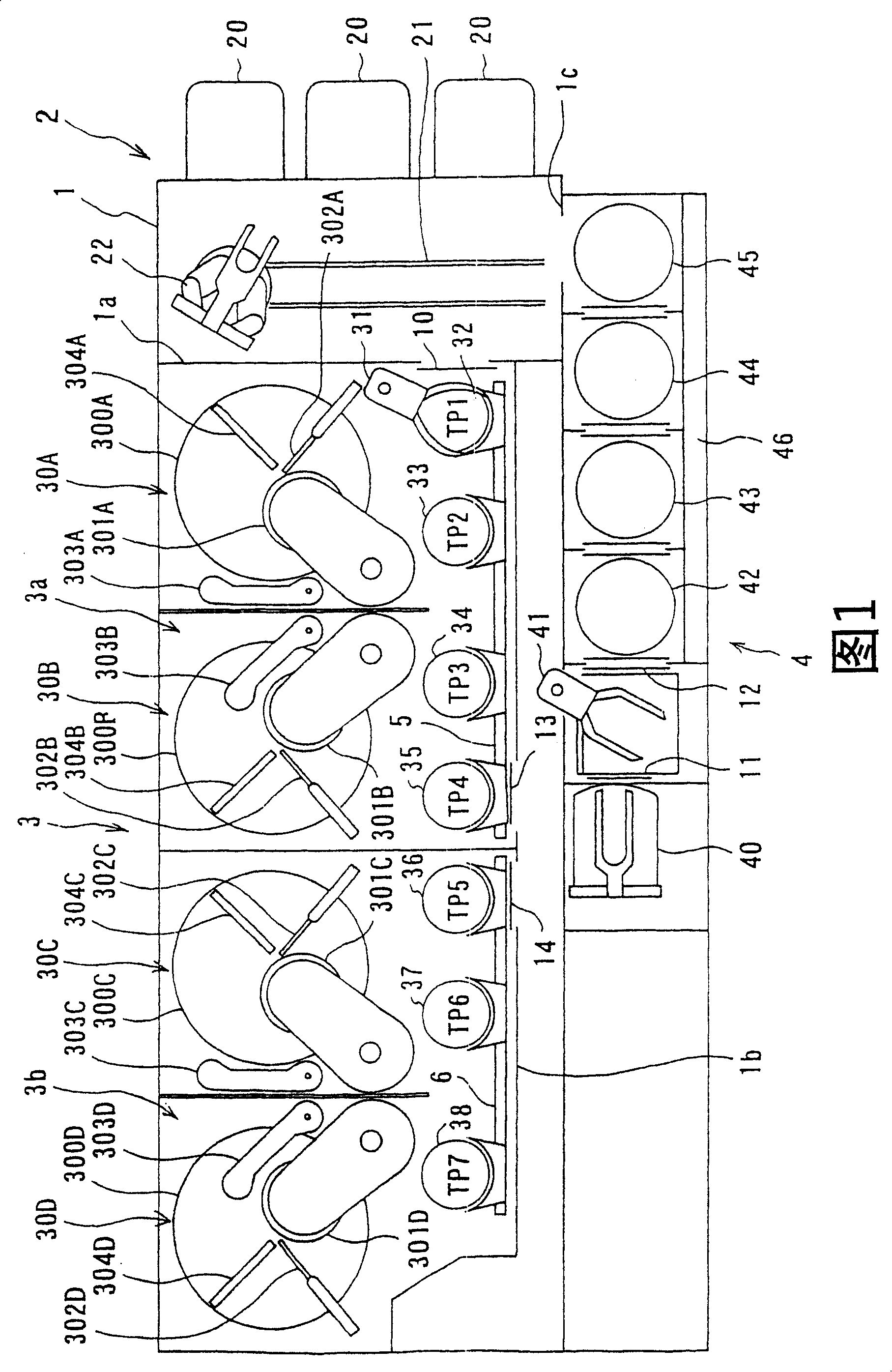
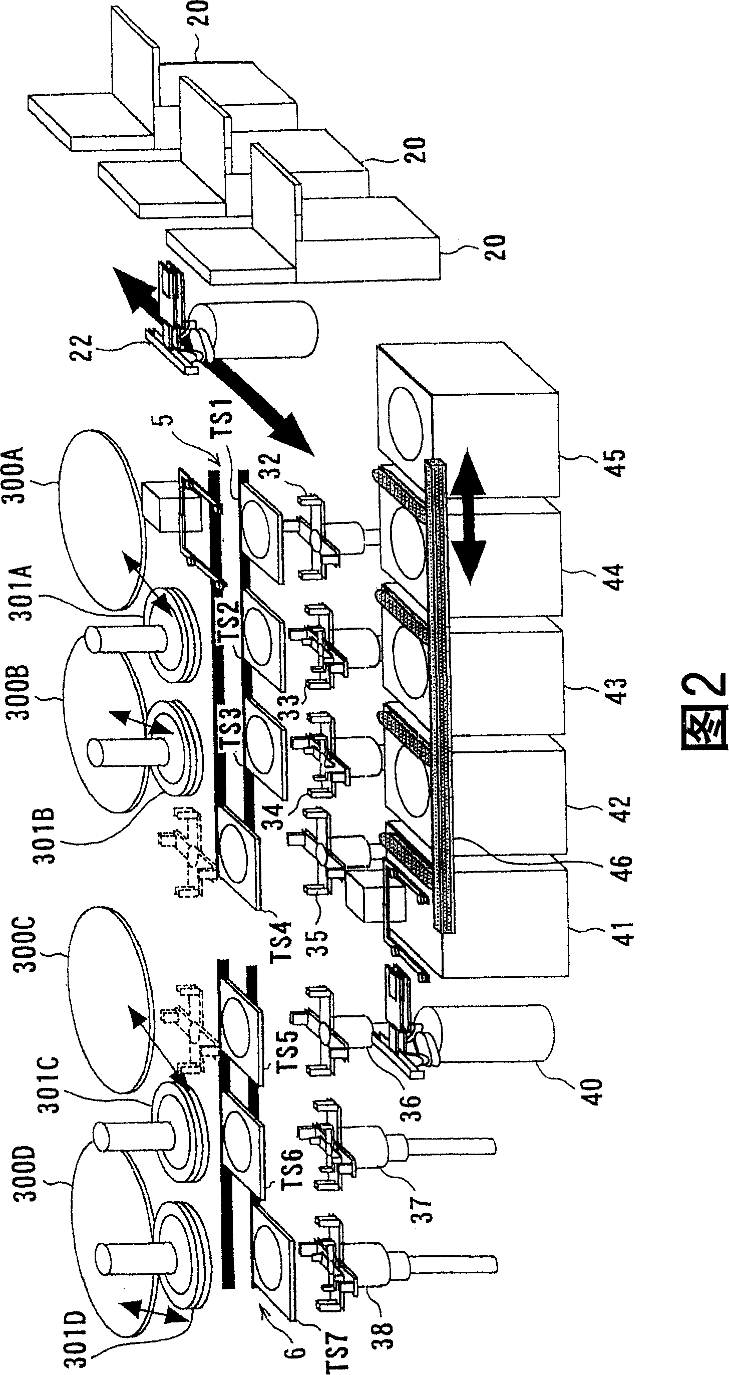
[0080] Next, an embodiment of the polishing device according to the present invention will be described in detail with reference to the accompanying drawings. 1 is a plan view showing the overall structure of a polishing apparatus according to an embodiment of the present invention, and FIG. 2 is a perspective view showing an outline of the polishing apparatus shown in FIG. 1 . As shown in Figure 1, the polishing device of the present embodiment is equipped with a substantially rectangular casing 1, and the loading / unloading section 2 and the grinding section 3 (3a) are divided by partition walls 1a, 1b, 1c in the inside of the casing 1. , 3b) and cleaning section 4. The loading / unloading unit 2, the grinding units 3a, 3b, and the cleaning unit 4 are independently assembled and exhausted independently.

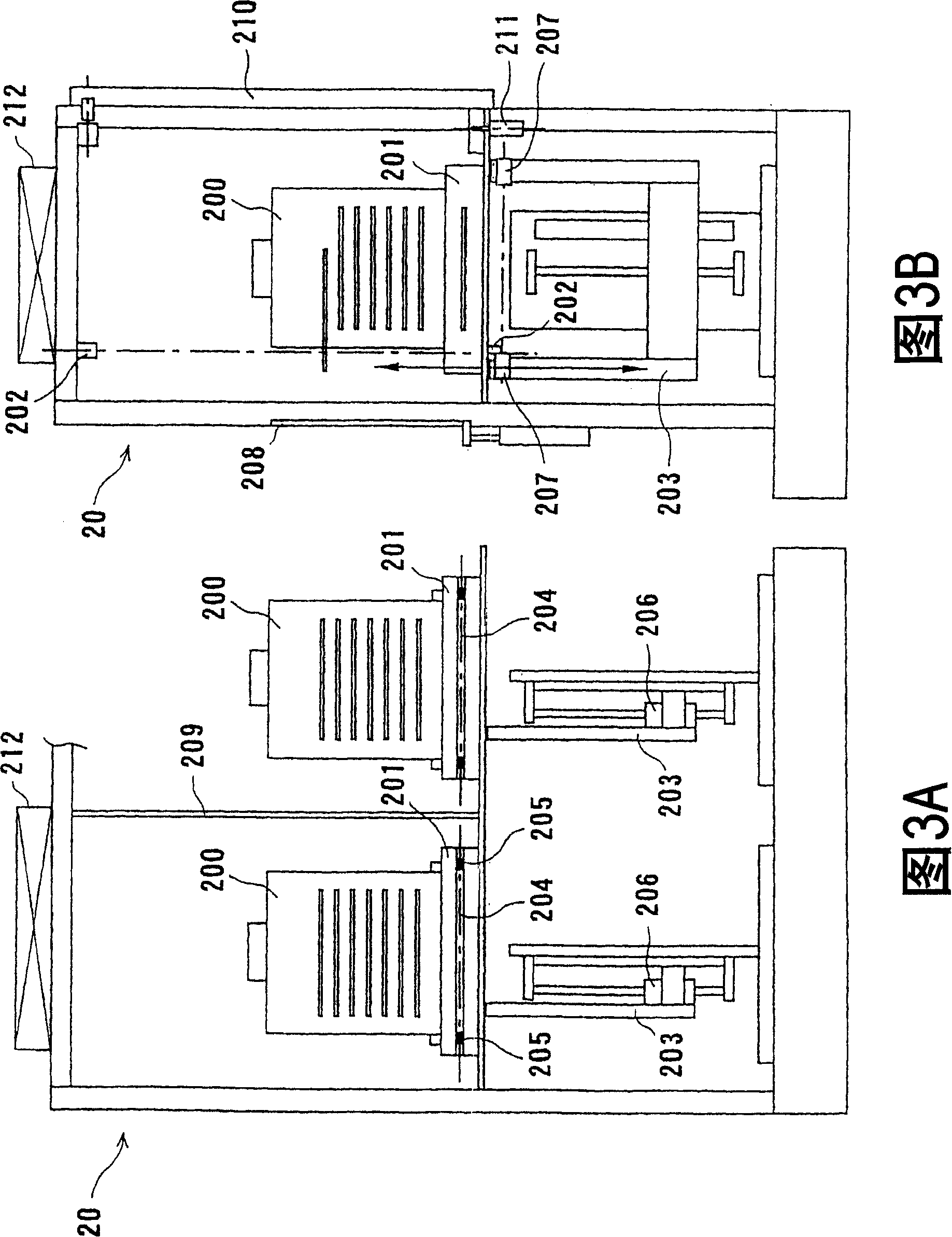
[0081] The loading / unloading section 2 includes two or more (not three in the present embodiment) front loading sections 20 on which wafer cassettes stacking a plurality of s...


PUM


Abstract

The present invention relates to a polishing apparatus having a plurality of polishing units (30A-30D). Moving mechanisms for moving top rings (301A SIMILAR 301D) between polishing positions on the polishing surfaces and wafer receiving / delivering positions are provided in each of the polishing units. Linear transporters (5, 6) are provided for transferring the wafer between a plurality of transferring positions (TP1-TP7) including the wafer receiving / delivering positions. Pushers (33, 34, 37, 38) for receiving and delivering the wafer between the linear transporters (5, 6) and the top rings (301A-301D) are provided at the transferring positions (TP2, TP3, TP6, TP7) as the wafer receiving / delivering positions.

Description

technical field [0001] The present invention relates to a substrate processing apparatus, and more particularly, to a polishing apparatus for polishing a polishing object such as a semiconductor wafer (wafer) into a flat and mirror-like surface. Background technique [0002] In recent years, with the progress of high integration of semiconductor devices, the wiring of circuits has been miniaturized, and the distance between wirings has become narrower and narrower. In particular, in the case of lithography with a line width of 0.5 μm or less, since the depth of focus becomes shallow, it is necessary to secure the flatness of the imaging surface of a stepper. A polishing apparatus that performs chemical mechanical polishing (CMP) is known as one means for flattening the surface of such a semiconductor wafer. [0003] This chemical mechanical polishing (CMP) apparatus includes a polishing table with a polishing cloth on it and a top ring. At the same time, the object to be p...

Claims


Application Information

Patent Timeline
Patent Type & Authority Patents(China)
IPC IPC(8): H01L21/304B24B37/04C23F1/00H01L21/00H01L21/677H01L21/68H01L21/687
CPCH01L21/67745B24B37/345H01L21/68707H01L21/67751H01L21/67219H01L21/67766H01L21/304H01L21/68
Inventor 若林聪户川哲二小菅隆一阿藤浩司外崎宏
Owner EBARA CORP
Features
  • R&D
  • Intellectual Property
  • Life Sciences
  • Materials
  • Tech Scout
  • Unparalleled Data Quality
  • Higher Quality Content
  • 60% Fewer Hallucinations
Learn More