Image display device
An image display device and a technology of a display part, which is applied to identification devices, lighting devices, static indicators, etc., can solve problems such as affecting image quality and compromising the stability of luminous brightness, and achieve the effect of stabilizing luminous brightness
- Summary
- Abstract
- Description
- Claims
- Application Information
AI Technical Summary
Problems solved by technology
Method used
Image
Examples
Embodiment 1
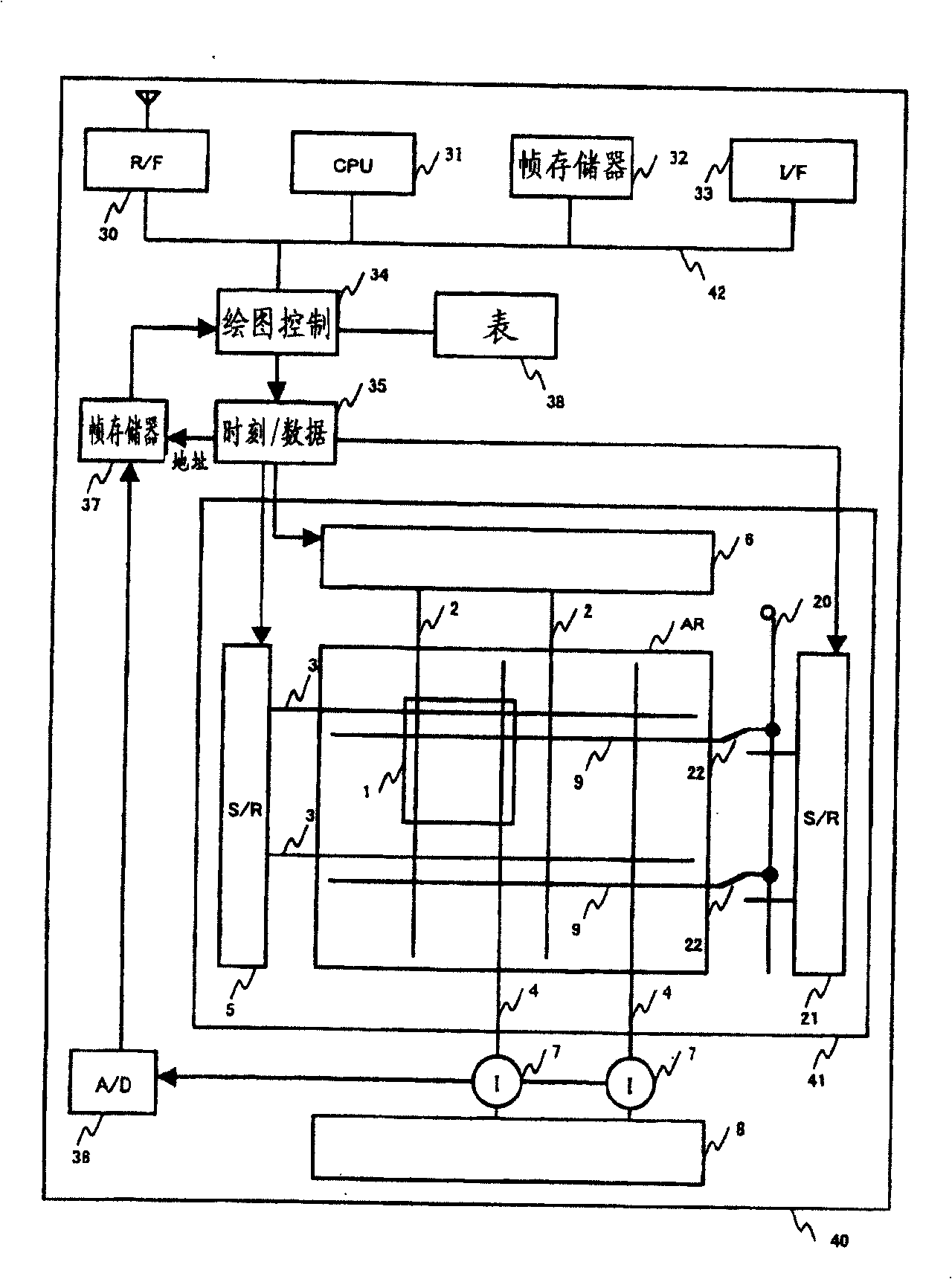
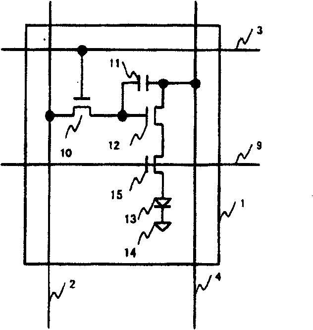
[0039] figure 1 It is a configuration diagram of the portable terminal 40 for explaining the first embodiment of the image display device of the present invention. The pixels 1 are arranged in a matrix along rows and columns and arranged in the display area AR. The signal line 2 , the gate line 3 , the power line 4 and the lighting control line 9 are respectively connected to the pixel 1 . In fact, there are a plurality of pixels 1 in the display area AR, but in order to simplify the drawings, in figure 1Only one pixel is shown in . One end of the signal line 2 is connected to a signal voltage input circuit 6 . One end of the gate line 3 is connected to the first shift register circuit 5 . One end of the power supply line 4 is connected to a power supply circuit 8 through a current measurement circuit 7 . One end of the lighting control line 9 is connected to the second shift register circuit 21 through the lighting switching switch 22 , and the other end of the lightin...
Embodiment 2
[0054] Below, use Figure 5-9 Example 2 of the present invention will be described. The basic structure and operation of the portable terminal applying the second embodiment are the same as the first embodiment already described, and the only difference between the second embodiment and the first embodiment lies in the pixel circuit and its driving system arranged on the glass substrate. Therefore, here we only focus on the pixel circuit part, explaining its structure and operation.
[0055] Figure 5 It is a configuration diagram around pixels of a portable terminal for explaining the second embodiment of the present invention. The pixels 1A are arranged in a matrix in the display area AR. The signal line 2, the reset line 53, the power line 4, and the lighting control line 9 are respectively connected to the pixel 1A. In fact, there are a plurality of pixels 1A in the display area AR, but in order to simplify the drawings, in Figure 5 Only one pixel is shown in . One ...
Embodiment 3
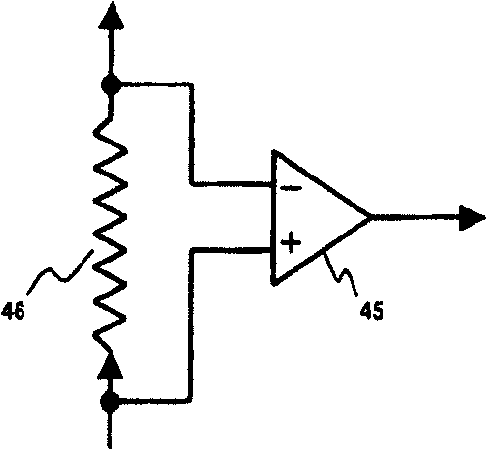
[0074] Below, use Figure 10 , 11 , to illustrate Embodiment 3 of the present invention. The basic structure and operation of the portable terminal according to Embodiment 3 of the present invention are the same as those of Embodiment 1 described above. Compared with Embodiment 1, Embodiment 3 differs only in the current measurement circuit and its driving system. Therefore, here we only focus on the part of the current measurement circuit, explaining its structure and operation.
[0075] Figure 10 It is a diagram illustrating the structure around pixels of a mobile terminal according to Embodiment 3 of the present invention. The pixels 1B are arranged in a matrix in the display area AR, and the signal lines 2 , gate lines 3 , power lines 4 and lighting control lines 9 are respectively connected to the pixels 1B. In fact, there are a plurality of pixels 1B in the display area AR, but in order to simplify the drawings, in Figure 10 Only one pixel is shown in . One end o...
PUM
 Abstract
Description
Claims
Application Information


