Chip encapsulation structure
A chip packaging structure and chip technology, which is applied in the direction of semiconductor/solid-state device parts, semiconductor devices, electrical components, etc., can solve the problem of offset or fracture of the third bonding wire, and achieve the effect of reducing the volume
- Summary
- Abstract
- Description
- Claims
- Application Information
AI Technical Summary
Problems solved by technology
Method used
Image

Examples
Embodiment Construction
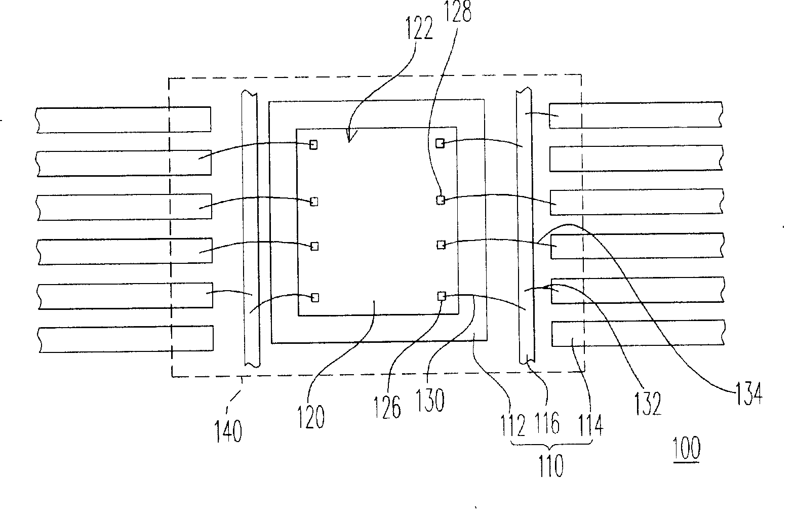
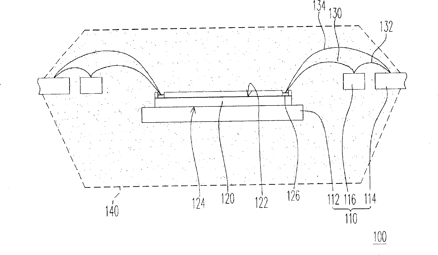
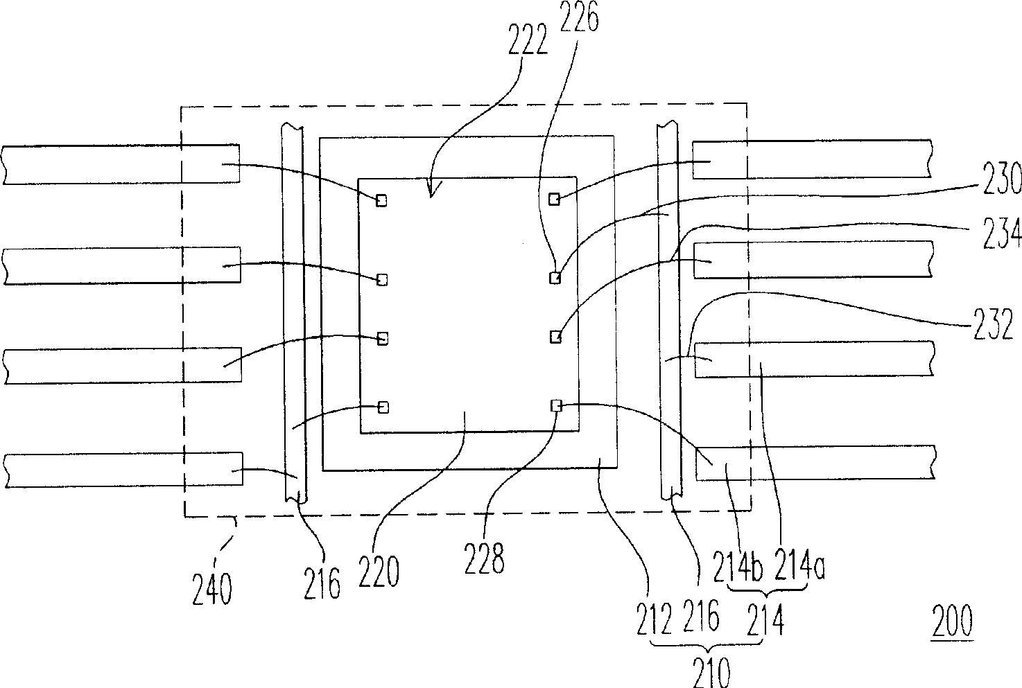
[0023] image 3 is a schematic side view of a chip package according to an embodiment of the present invention. Figure 4 yes image 3 A schematic top view of the chip package. For the convenience of explanation, image 3 and Figure 4 is a perspective view of the encapsulant 240 , and only outlines of the encapsulant 240 are drawn with dotted lines. The chip packaging structure 200 includes a lead frame 210 , a chip 220 , at least one first bonding wire 230 , at least one second bonding wire 232 , a plurality of third bonding wires 234 and an encapsulant 240 .
[0024] The lead frame 210 includes a chip holder 212 , a plurality of inner leads 214 and a bus bar 216 . The inner pins 214 are disposed on the periphery of the chip holder 212 , wherein the inner pins 214 include at least one first inner pin 214 a and a plurality of second inner pins 214 b. The bus bar 216 is interposed between the die holder 212 and the inner lead 214 , and the bus bar 216 maintains a first h...
PUM
 Abstract
Description
Claims
Application Information