Method for measuring Cube-Prism non-orthogonality angle and scale factor correct value
A scaling and non-orthogonal technology, which is applied in the field of semiconductor manufacturing, can solve problems such as limitations in the use of lithography machines, and achieve the effect of simple marking design
- Summary
- Abstract
- Description
- Claims
- Application Information
AI Technical Summary
Problems solved by technology
Method used
Image
Examples
Embodiment Construction
[0026] A method for measuring the non-orthogonal angle of a square mirror and the correction value of the scaling factor of the present invention will be described in detail below in conjunction with specific embodiments.
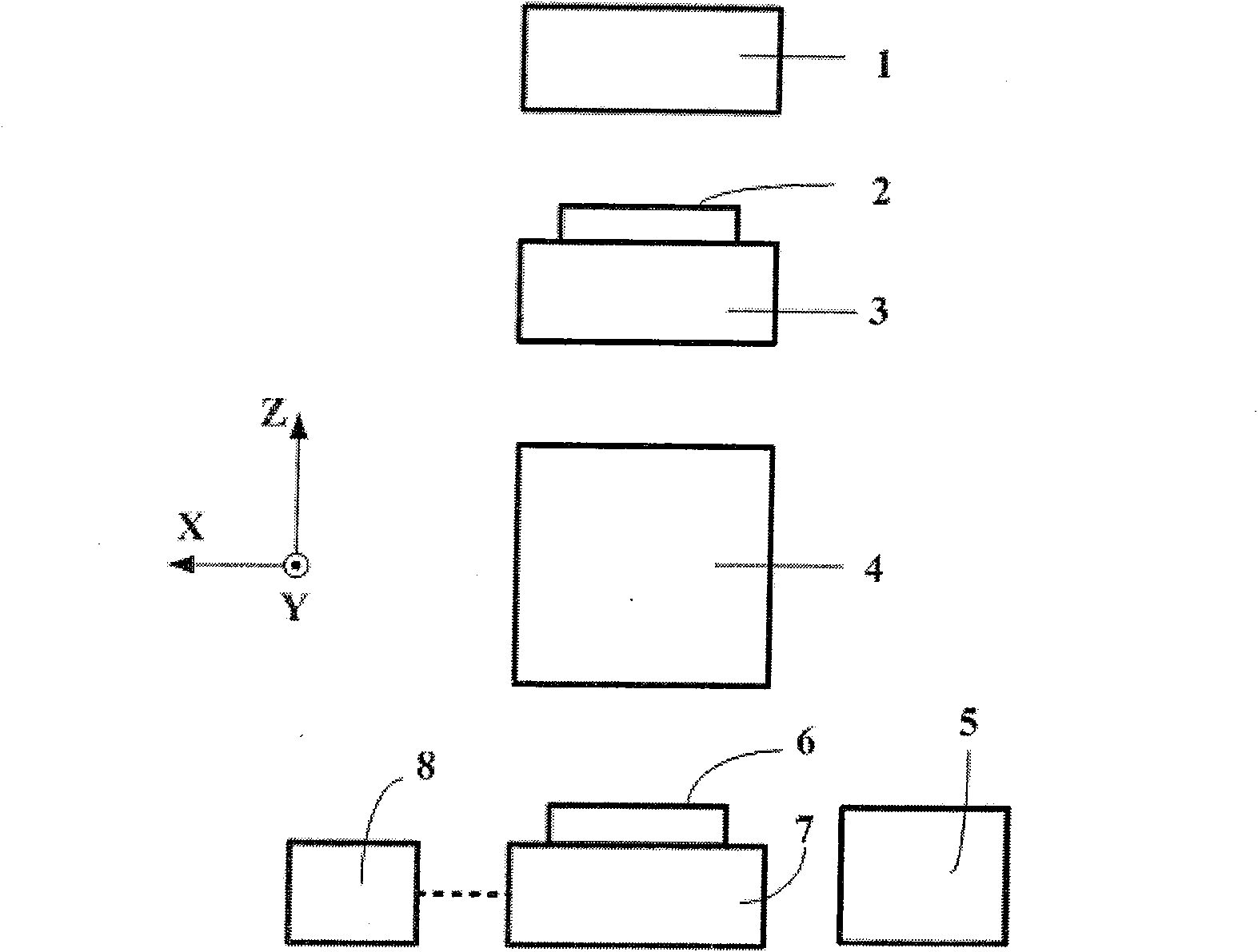
[0027] Wherein the lithography machine system used in the present invention for exposure and alignment measurement is as figure 2 As shown, it includes: an illumination system 1, a mask stage 3 carrying a mask 2, an optical system 4 for mask imaging, a workpiece stage 7 carrying a silicon wafer 6, an alignment system 5 for off-axis alignment, An X-direction interferometer 8 and a Y-direction interferometer for monitoring the movement position of the workpiece table.
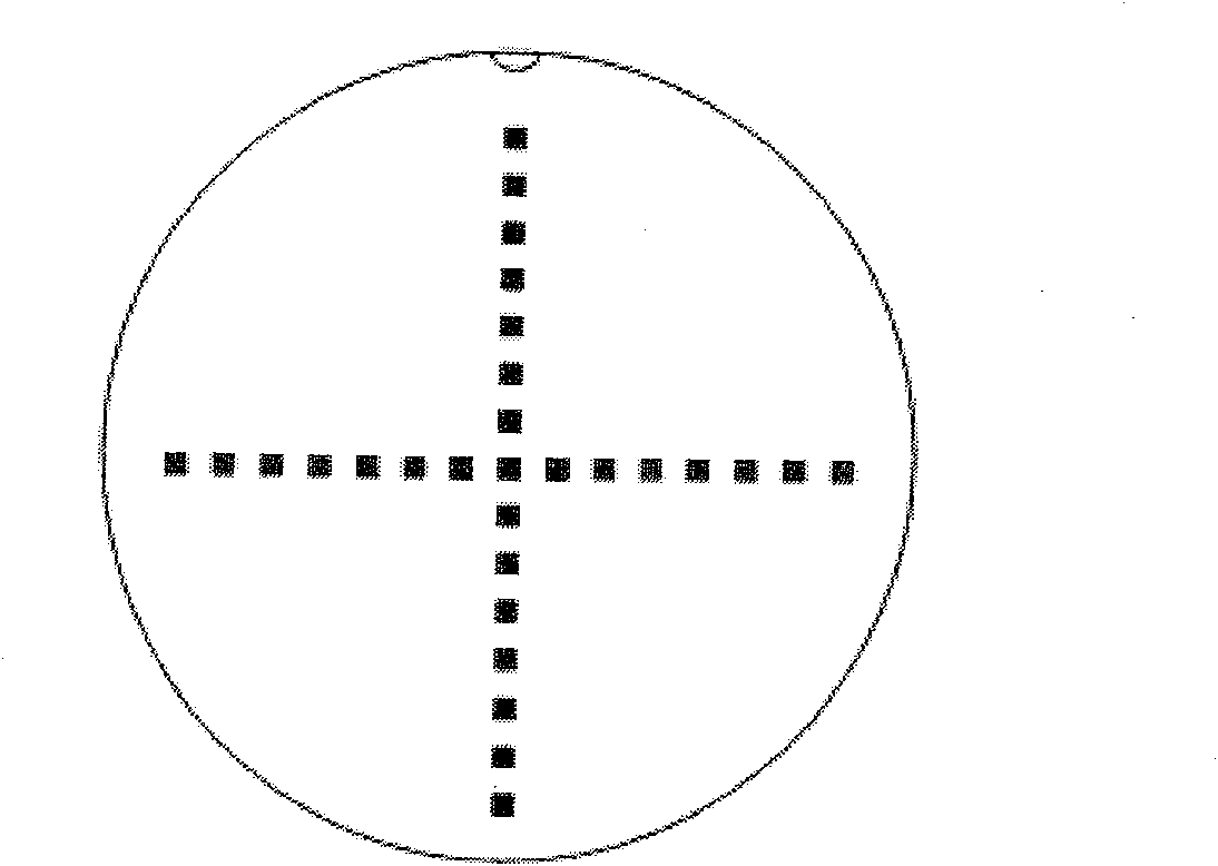
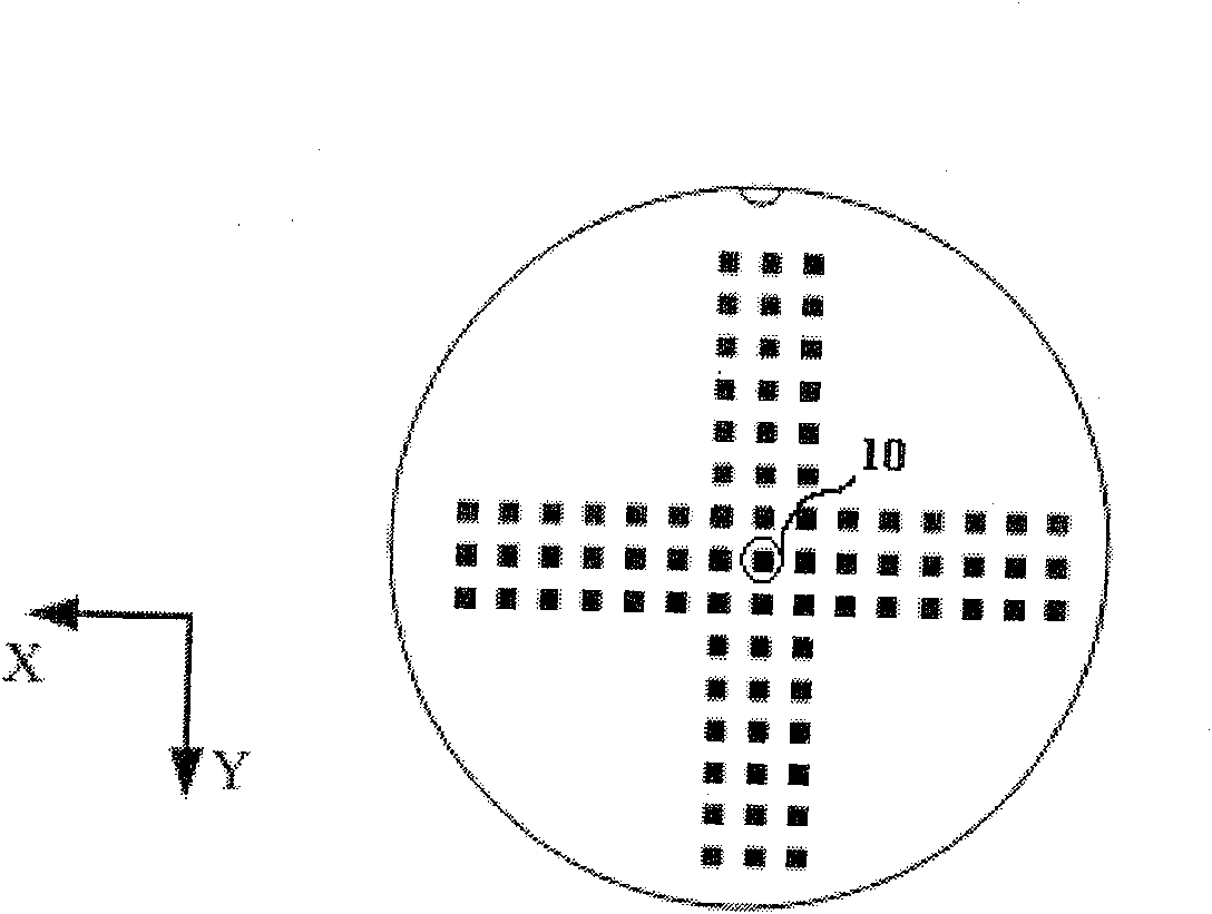
[0028] In the present invention, two alignment marks on the mask are used for exposure, mark A and mark B, mark A and mark B are off-axis alignment marks of the same type, which measure the square mirror non-orthogonality angle and the scaling factor correction value The specific steps are: ...
PUM
 Abstract
Description
Claims
Application Information


