Electric connection structure of circuit board and the circuit board possessing the connection structure

A circuit board and conductive structure technology, which is applied to printed circuit components, electrical connection printed components, printed circuits connected to non-printed electrical components, etc., can solve the problems that cannot be effectively reduced, decoupling capacitance loses decoupling, etc.

CN100592842CActive Publication Date: 2010-02-24IND TECH RES INST
6 Cites 0 Cited by

Patent Information

Authority / Receiving Office
CN · China
Patent Type
Patents(China)
Current Assignee / Owner
Publication Date
2010-02-24

Smart Images

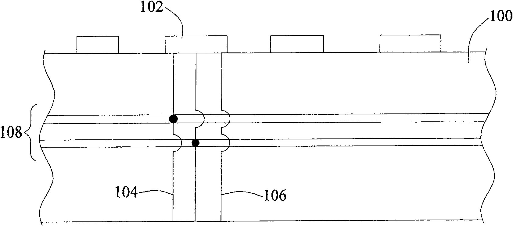
  • Figure 1
    Figure 1
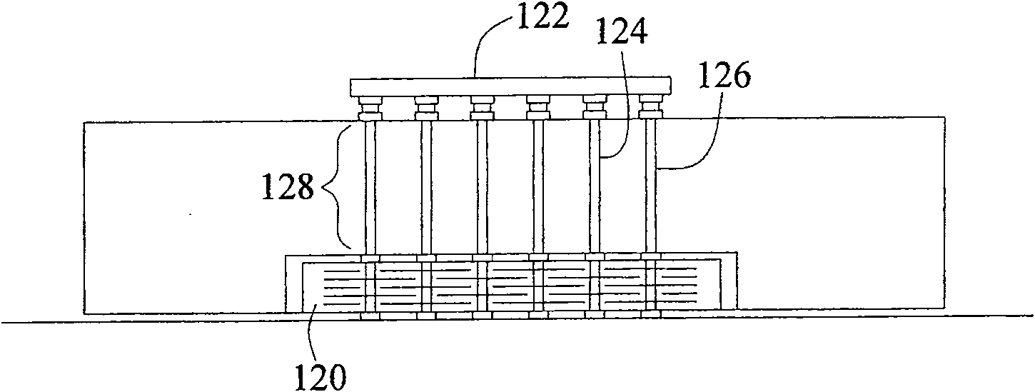
  • Figure 2
    Figure 2
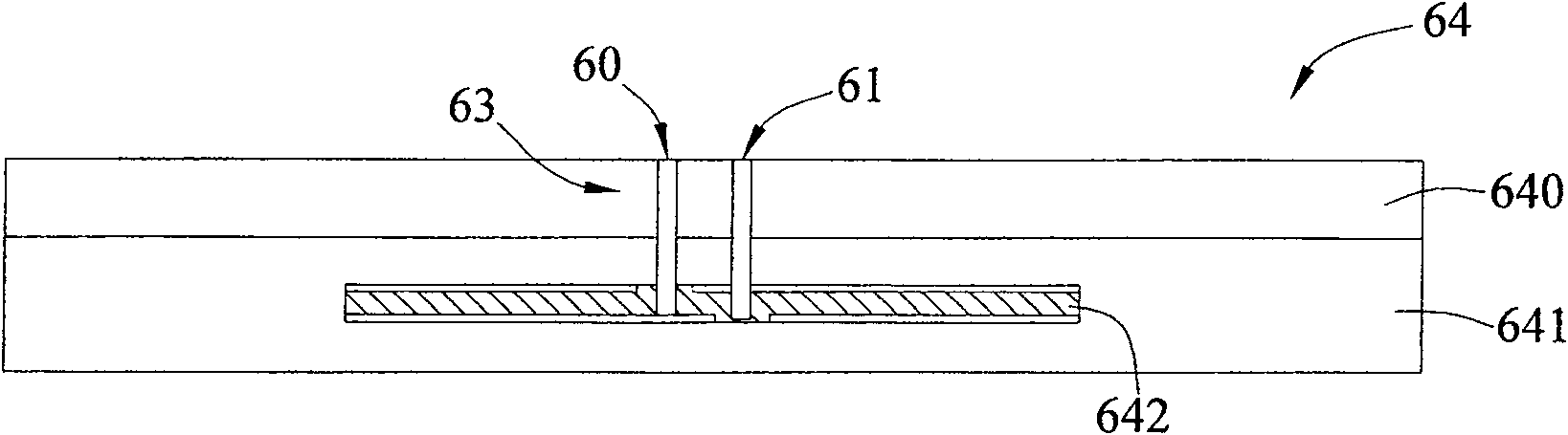
  • Figure 3
    Figure 3
Patent Text Reader

Abstract

The present invention discloses a electronic connection structure of circuit board and a circuit board thereof, which comprises the following procedures: connecting power contact and grounding contactof electronic component to power plane and ground plane of circuit board separately; electronic connection structure comprises the first conductive structure and the second conductive structure, oneend of both conductive structure is conductive contact segment, two conductive contact segments electronically connect with power contact and ground separately, the other end of each conductive structure extends from its conductive contact segment to form a plurality of dual segments, the two dual segments of the two conductive structure are pair configuration. The pairing dual segments of the twoconductive structures deploy in the way of interleaved array to form loop with two current in opposite direction. Magnetic flux is counteracted mutually to make situation that impedance of decouplingcapacitor in electronic circuit power supply system adds along with the rise of electronic component switching frequency eases up.
Need to check novelty before this filing date? Find Prior Art

Description

technical field

[0001] The present invention relates to an electrical communication structure of a circuit board, in particular to a metal communication structure arranged in the circuit board for electrically connecting the contacts of the electronic components on the circuit board to the power supply layer and the grounding layer of the circuit board. structure, this circuit board can be a circuit board with embedded capacitors. Background technique

[0002] Electronic components are often arranged on a printed circuit board (Printed Circuit Board) or an integrated circuit substrate (IC substrate) (the circuit board is used as an example below, but not limited to the circuit board). The metal connection structure in the circuit board is electrically connected to the power plane (Power plane, also known as the power plane) and the ground plane (Ground plane, also known as the ground plane) in the circuit board, so that the electronic component can receive power from the cir...

Examples

Embodiment Construction

[0081] Please also refer to Figure 5 , Figure 6 and Figure 7 , which is a structural schematic diagram of the first embodiment of the electrical connection structure of the present invention, wherein Figure 6 is a three-dimensional structure diagram of the first embodiment, Figure 5 it's for Figure 6 top view of the , while Figure 7 It is a structural diagram of the first embodiment actually configured in the circuit board 300, and its representation is for the first embodiment in Figure 5 The sectional view of position 7-7 in the center is expressed by taking a 90-degree section and turning the section area at a 90-degree angle to form a plane.

[0082] Please mainly use Figure 7 match Figure 5 and Figure 6 After reading, it can be seen from the figure that the electrical connection structure 200 of the first embodiment is to electrically connect at least one power contact 91 and at least one ground contact 92 of the electronic component 90 to the power pla...