Implementing method and device of optical modulation
An implementation method and technology of optical modulation, applied in the field of optical modulation, can solve the problems of increased bit error rate due to bit errors, and achieve high reliability, cost saving, and easy-to-implement effects
- Summary
- Abstract
- Description
- Claims
- Application Information
AI Technical Summary
Problems solved by technology
Method used
Image

Examples
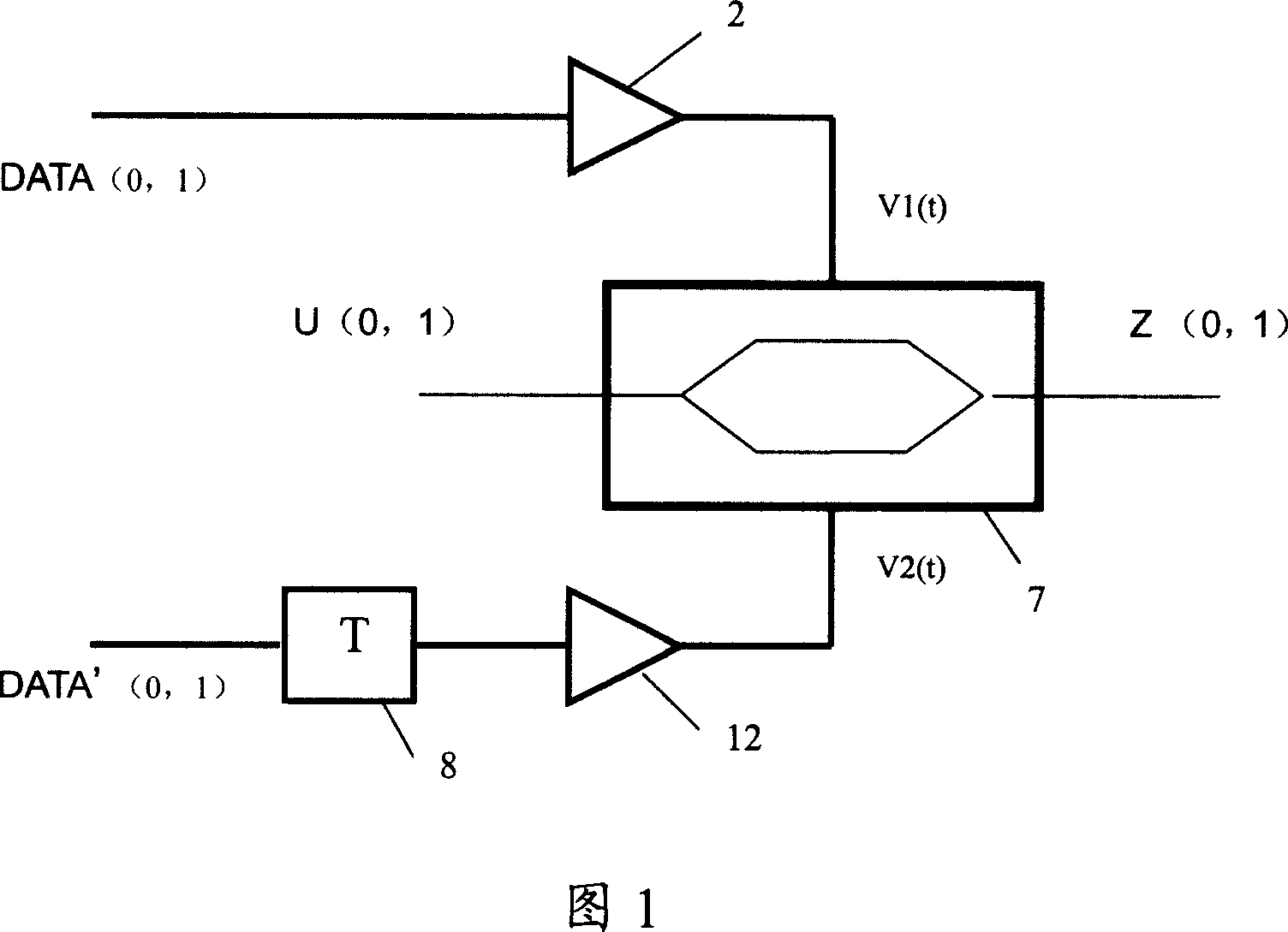
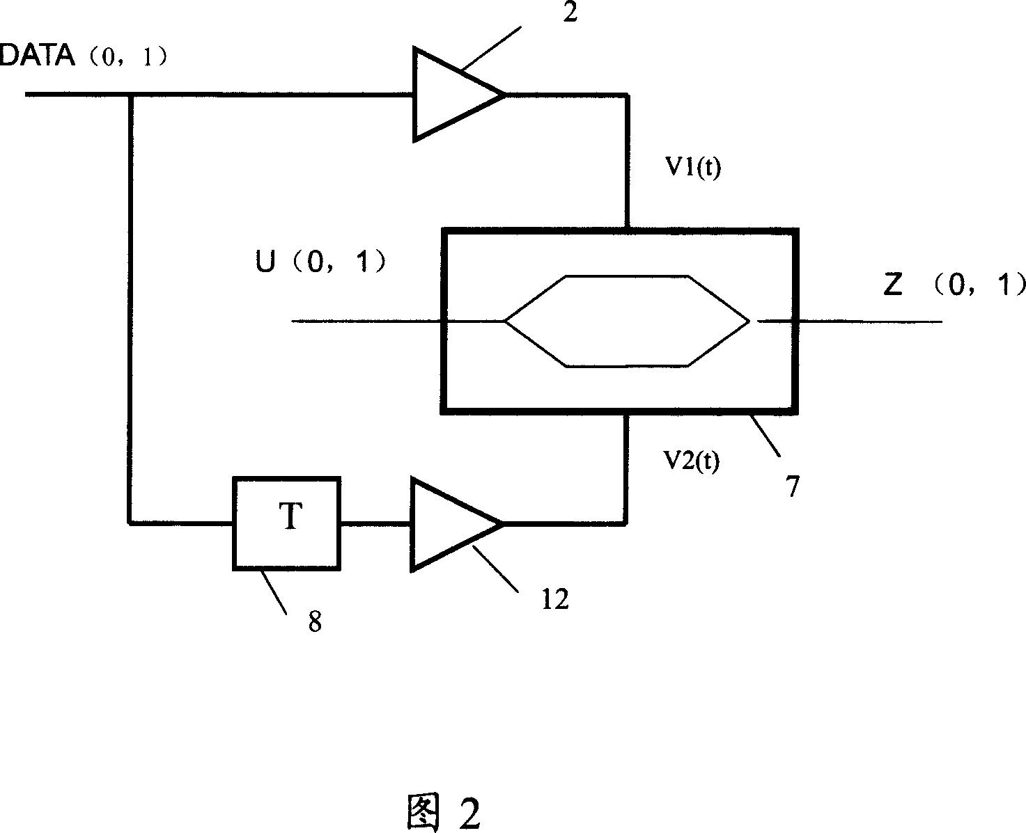
Embodiment 1
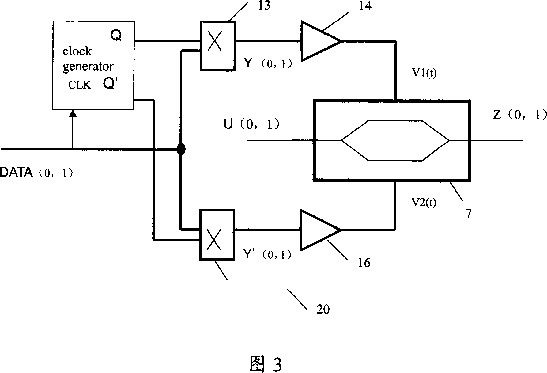
[0056] The clock generator in the second embodiment of the present invention uses the associated clock signal to generate the required clock sequence, so that when the input electrical signal data stream DATA(0, 1) passes through the clock generator, two complementary clock signals are generated. Compared with Embodiment 1 of the present invention, the advantage of this clock generator is that it can realize more clock sequences in various states as required.
[0057] Clock generator 2 in Fig. 5 has two input ports: data signal input end I and clock signal input end CLK, and two output ports Q and Q', wherein two output ports Q and Q' output complementary, its work The principle is illustrated by taking T flip-flop as an example, as shown in Figure 6.
[0058] 6, the clock signal 11 is input to the clock signal input terminal CLK of the T flip-flop, and the input electrical signal data stream 1 is input to the data signal input terminal I of the T flip-flop. When the input da...
PUM
 Abstract
Description
Claims
Application Information
 - R&D
- Intellectual Property
- Life Sciences
- Materials
- Tech Scout
- Unparalleled Data Quality
- Higher Quality Content
- 60% Fewer Hallucinations
Browse by: Latest US Patents, China's latest patents, Technical Efficacy Thesaurus, Application Domain, Technology Topic, Popular Technical Reports.
© 2025 PatSnap. All rights reserved.Legal|Privacy policy|Modern Slavery Act Transparency Statement|Sitemap|About US| Contact US: help@patsnap.com