
Packaging structure

A packaging structure and carrier technology, applied in electrical components, electrical solid devices, circuits, etc., can solve problems such as poor heat dissipation

Active Publication Date: 2007-11-14
CYNTEC
View PDF0 Cites 5 Cited by
  • Summary
  • Abstract
  • Description
  • Claims
  • Application Information

AI Technical Summary

Problems solved by technology

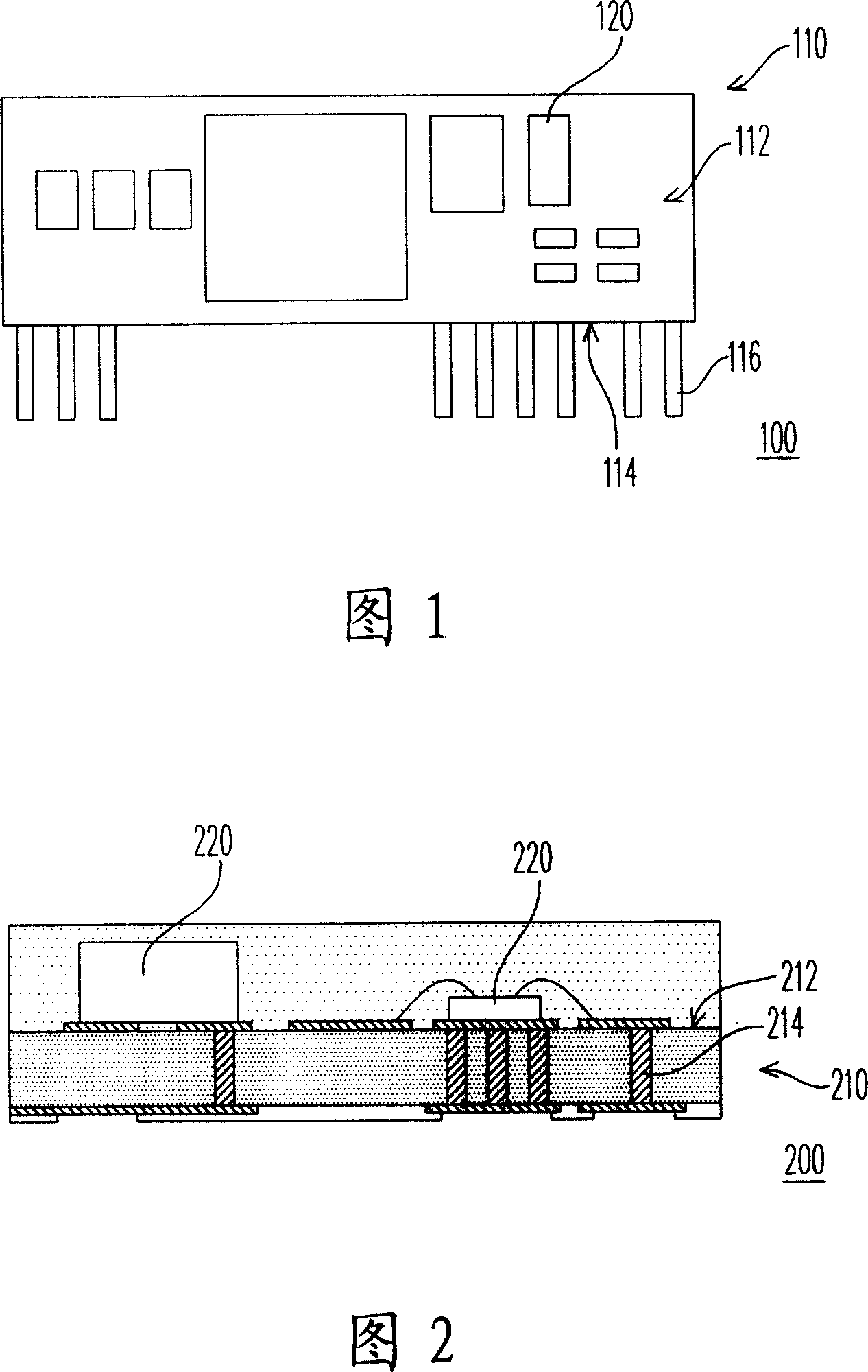
[0005] Although the existing packaging structure 200 has the advantages of high component configuration density, small volume, simple manufacturing process, low cost, and can be placed in the next level of electronic devices in an automated manner; , the heat can only be transferred to the wires of the next-level electronic device in the form of conduction through the conductive via 214 in the packaging substrate 210
Therefore, the heat dissipation (capacity of heat dissipation) of the existing package structure 200 is relatively poor.

Method used


Image

  • Packaging structure
  • Packaging structure
  • Packaging structure

Examples


no. 1 example

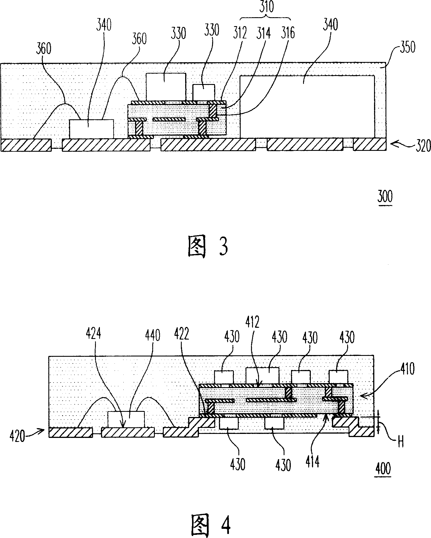
[0050] Please refer to FIG. 3 , which is a schematic cross-sectional view of the packaging structure according to the first embodiment of the present invention. The packaging structure 300 of the first embodiment includes a first carrier 310, a second carrier 320, at least one first electronic component 330 (for example, two are shown in FIG. 3 ) and at least one second electronic component 340 (FIG. 3 For example, two are shown). The second carrier 320 is electrically connected to the first carrier 310 , and the thermal resistance of the first carrier 310 may be greater than the thermal resistance of the second carrier 320 . The first electronic components 330 are disposed on the first carrier 310 and electrically connected to the first carrier 310 . The second electronic components 340 are disposed on the second carrier 320 and electrically connected to the second carrier 320 , and the heating power of each first electronic component 330 may be smaller than that of each sec...

no. 2 example

[0056] Please refer to FIG. 3 and FIG. 4 , wherein FIG. 4 is a schematic cross-sectional view of a package structure according to a second embodiment of the present invention. The main difference between the packaging structure 400 of the second embodiment and the packaging structure 300 of the first embodiment is that the first electronic components 430 can be disposed on the opposite surfaces 412 , 414 of the first carrier 410 . In the second embodiment, the first carrier 410 can still be configured on the second carrier 420 . The second carrier 420 has a first carrying area 422 and a second carrying area 424 , and the first carrying area 422 and the second carrying area 424 are not on the same plane. In other words, as far as the relative position shown in FIG. 4 is concerned, there is a height difference H between the second carrying area 424 and the first carrying area 422 . In addition, the first carrier 410 is disposed on the first carrying area 422 , and the second el...

no. 3 example

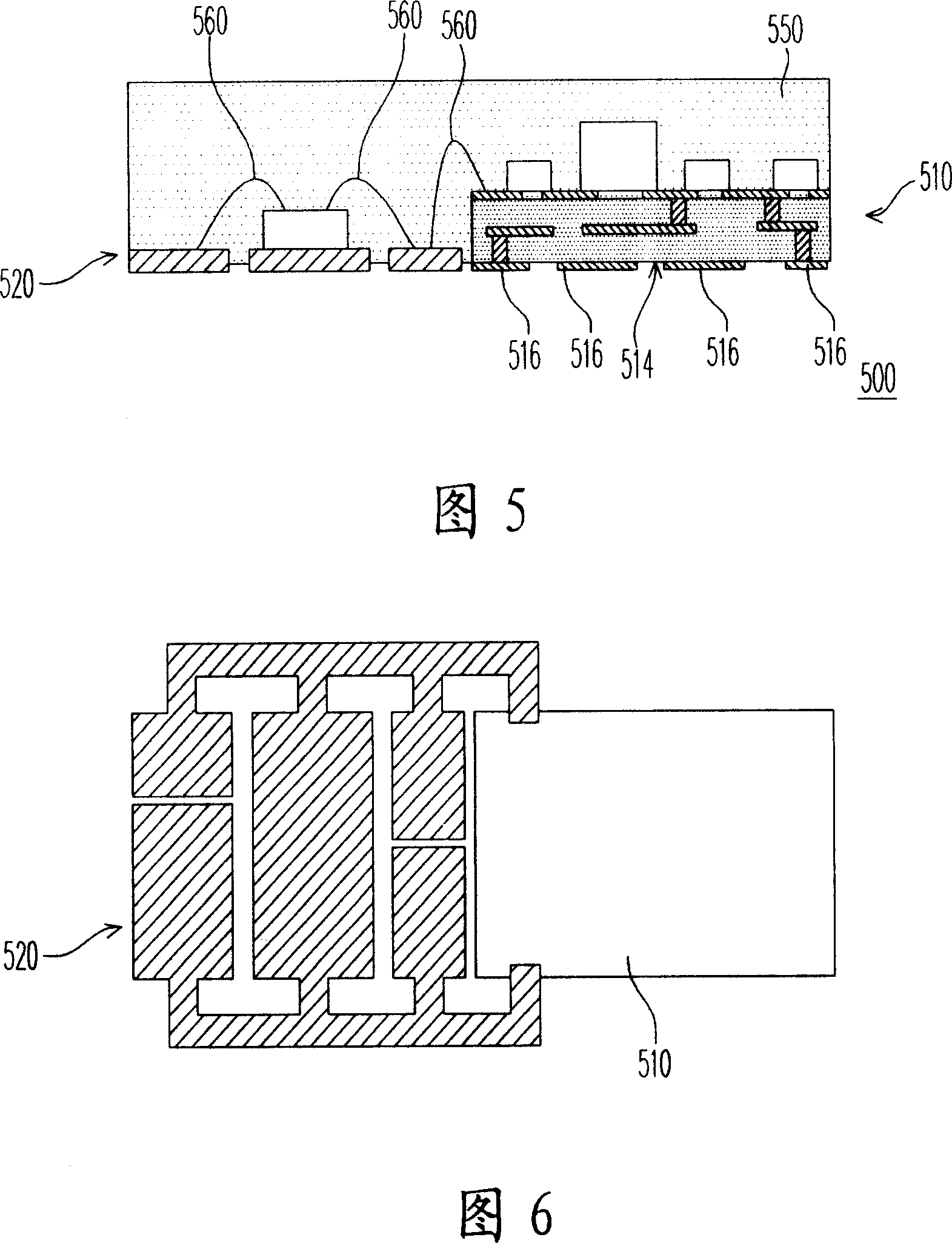
[0059] Please refer to FIG. 3 , FIG. 4 and FIG. 5 , wherein FIG. 5 is a schematic cross-sectional view of a packaging structure according to a third embodiment of the present invention. The main difference between the packaging structure 500 of the third embodiment and the packaging structures 300 and 400 of the above-mentioned embodiments is that the first carrier 510 of the third embodiment can be arranged beside the second carrier 520 . In addition, the package structure 500 further includes at least one bonding wire 560 (three wires are shown in FIG. 5 ), and the first carrier 510 is electrically connected to the second carrier 520 through at least one of these bonding wires 560 . In addition, the first carrier 510 may have a plurality of solder pads 516 disposed on a surface 514 of the first carrier 510 and exposed to the glue 550 . Compared with the above-mentioned embodiments, the solder pads 516 exposed from the glue 550 in the third embodiment can transmit electrical ...


PUM


Abstract

The invention is a packaging structure, comprising a first bearer, a second bearer, at least a first electronic component and at least a second electronic component, where the second bearer is connected with the first bearer; the first electronic component is arranged on and connected with the first bearer; and the second electronic component is arranged on and connected with the second bearer.

Description

technical field [0001] The present invention relates to a packaging structure, and more particularly to a packaging structure with multiple carriers. Background technique [0002] The packaging structure is a product formed after complicated packaging process steps. Various package structures have different electrical performance and capacity of heat dissipation. Therefore, designers can choose a package structure that meets their electrical performance and heat dissipation requirements according to their design requirements. [0003] Please refer to FIG. 1 , which shows a schematic diagram of a conventional packaging structure. The conventional package structure 100 includes a printed circuit board (printed circuit board, PCB) 110 and a plurality of electronic components 120 . The electronic components 120 are disposed on a surface 112 of the printed circuit board 110 and are electrically connected to the printed circuit board 110 . The printed circuit board 110 has a pl...

Claims


Application Information

Patent Timeline
Patent Type & Authority Applications(China)
IPC IPC(8): H01L25/00H01L23/488
CPCH01L2924/1305H01L2224/48091H01L2924/19107H01L2924/0002H01L2224/48227H01L2924/19105H01L2924/13091H01L2924/13055
Inventor 陈大容林逸程吕保儒方怡旻温兆均刘春条
Owner CYNTEC
Learn More