

Method of testing unloaded, large-area printed circuit boards with a finger tester
A technology for circuit boards and testers, which is applied in printed circuit testing, electronic circuit testing, non-contact circuit testing, etc., and can solve problems such as the development, production and operation of super-large probe testers, which are expensive and the number of testers is limited.
- Summary
- Abstract
- Description
- Claims
- Application Information
AI Technical Summary
Problems solved by technology
Method used
Image

Examples
Embodiment Construction
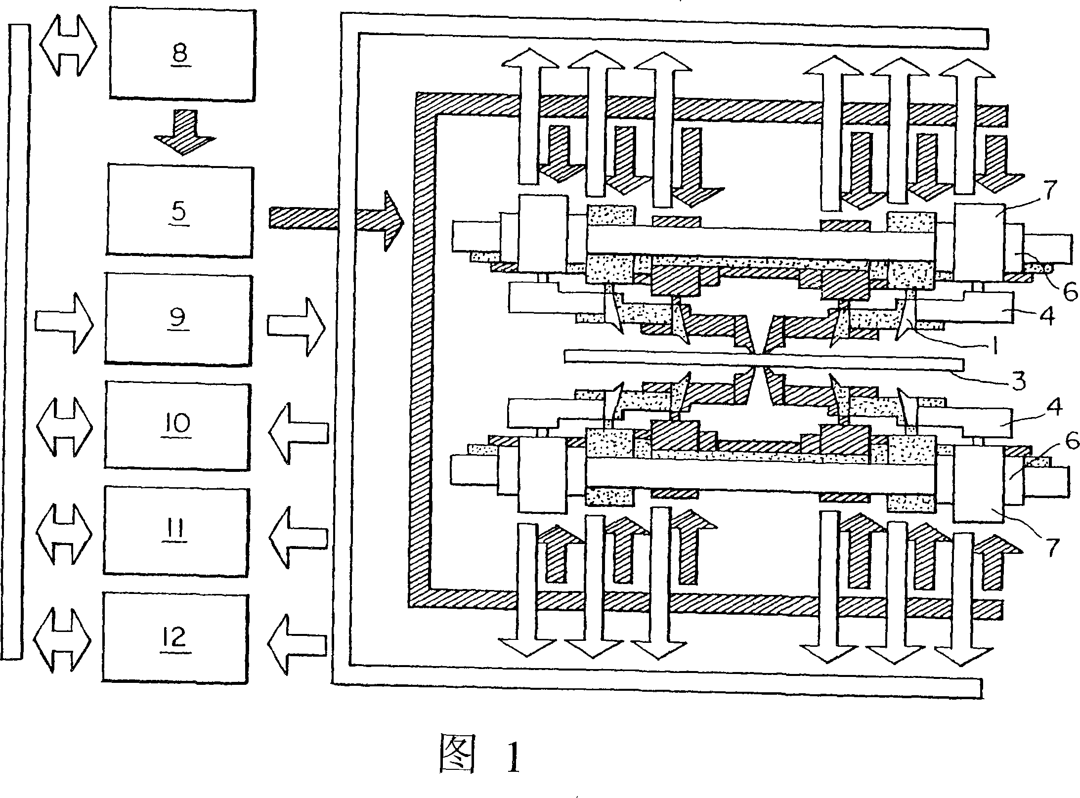
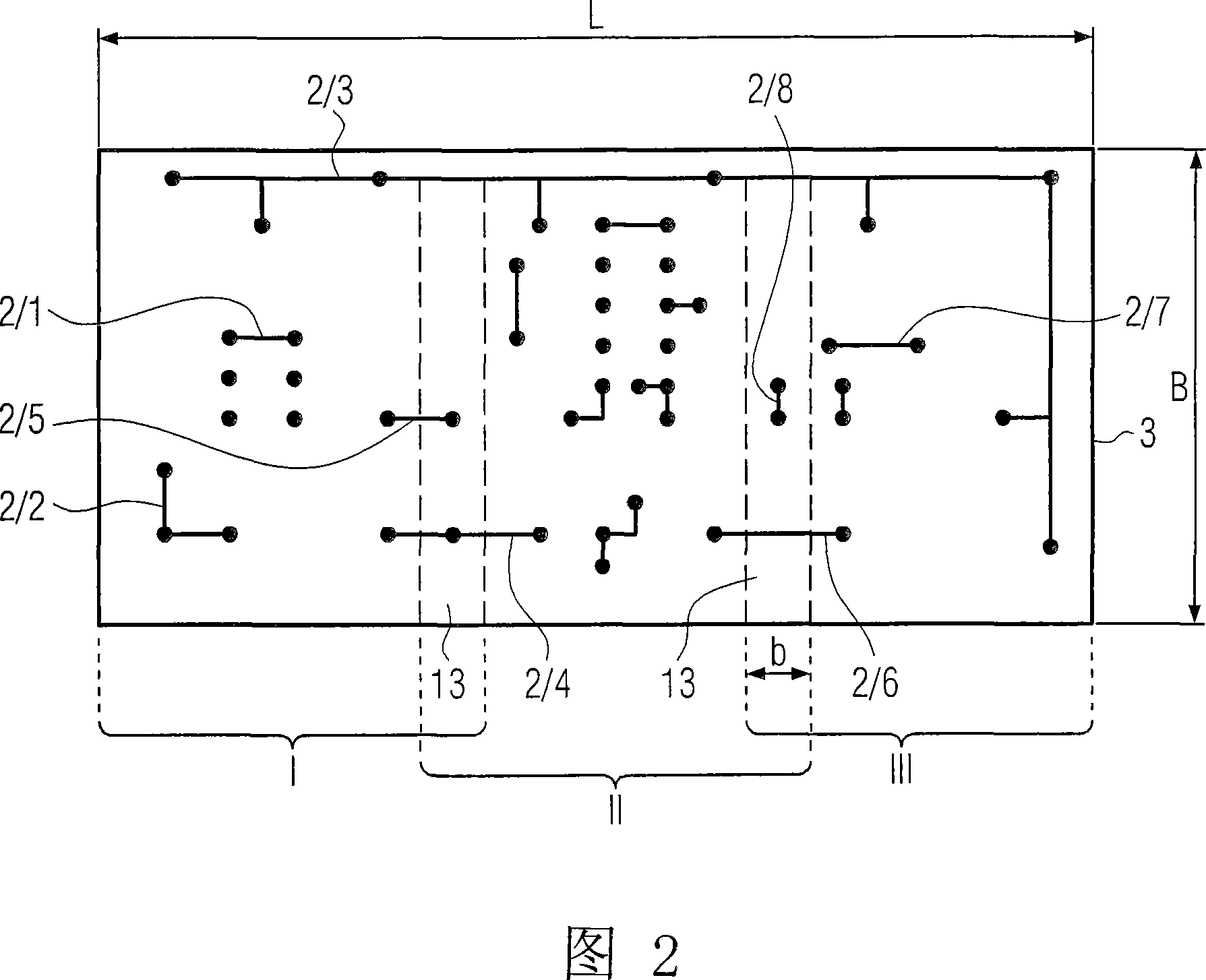
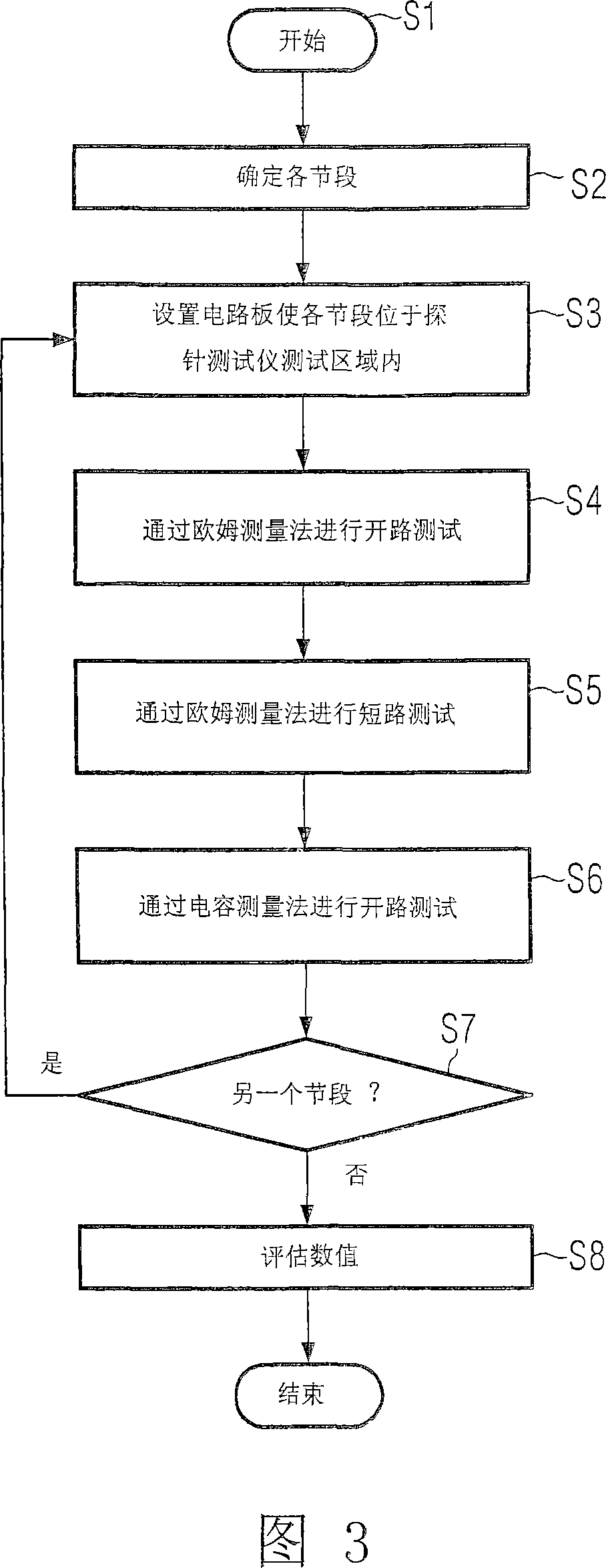
[0027] The method according to the invention for testing large, non-componentized circuit boards with conductor paths is carried out by means of a probe tester. The probe tester has several test electrodes 1 which can be brought into contact with the circuit board test points of the conductor paths 2 of the circuit board 3 (FIGS. 1, 2). Each test electrode 1 is integrated in a contact probe 4 . In this example, the probe tester contains a composite probe system, the composite probe system contains 12 contact probes 4 in total, and every 6 contact probes are placed on one side of the circuit board 3 to be tested on the side. EP0468135A1 discloses a pointer probe in which contact probes are independently movable relative to further contact probes. The contact probes 4 are movable parallel to the surface of the circuit board 3 so that the test electrodes 1 can be brought into contact with specific circuit board test points of the conductor paths. Each of said contact probes 4 ...
PUM
 Abstract
Description
Claims
Application Information