
Patsnap Eureka
For R&D, Patsnap Eureka makes reading and utilizing patents & technical documents easy.
Patsnap Eureka AIR
Designed for self-driven R&D workflows. Generate viable solutions, solve complex R&D challenges, empower your innovation with AI.

Patsnap Eureka Materials
Designed for material experts only. Revolutionize your material R&D, from search, analyze, to developing new materials.

TechResearch
Generate reliable direction feasibility study reports for your R&D in just a few steps.

TechSeek
Discover and master advanced knowledge NOW. Basics, ideas, possibilities, all at once.

TechMind
As an expert in R&D Theories, TechMind can generates customized viable solutions instantly.

TechRisk
Analyze your overall solution with one click, know your potential R&D risks in advance.

TechMonitor
Get weekly tech updates, stay abreast of the latest tech innovations and key insights.
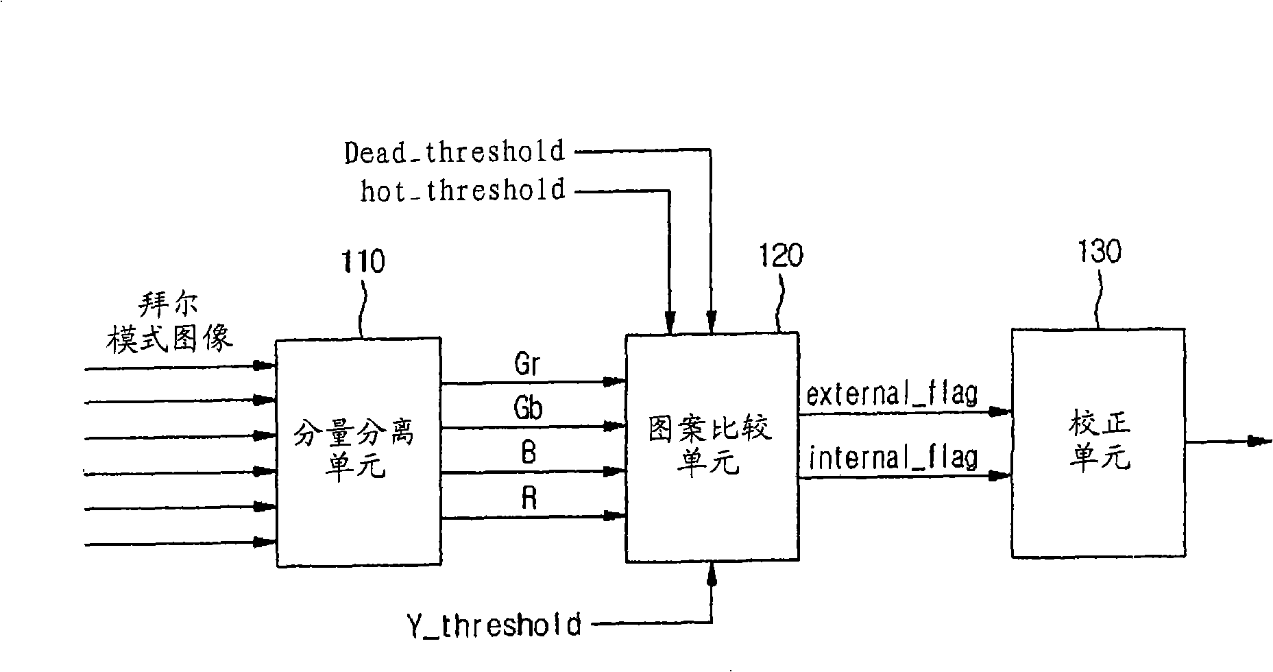
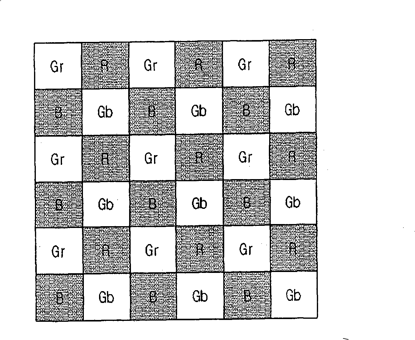
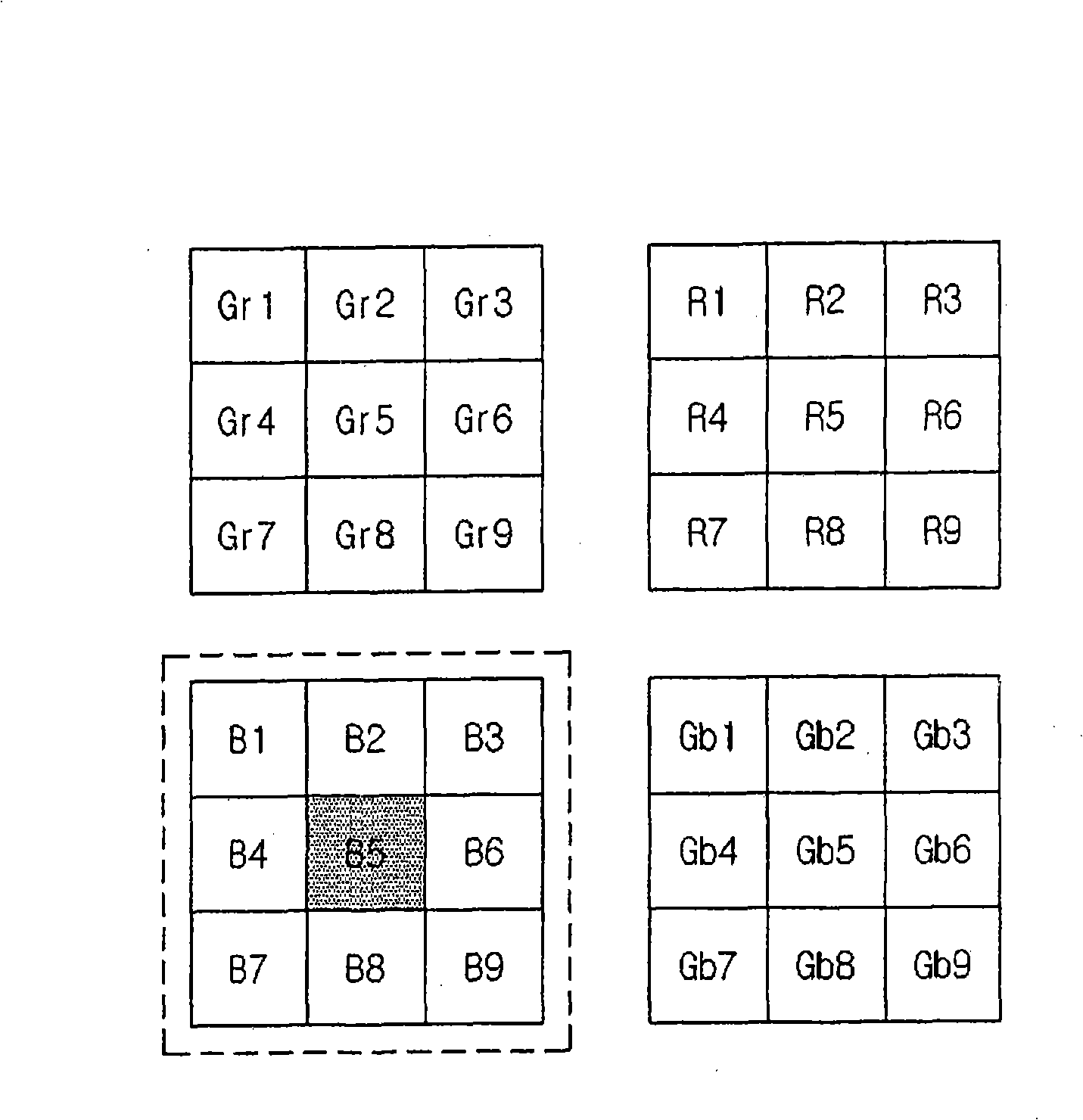
Device of processing dead pixel
A technology for processing devices and dead pixels, which is applied in the field of processing devices for bad pixels of image sensors, and can solve problems such as distortion
- Summary
- Abstract
- Description
- Claims
- Application Information
AI Technical Summary
Problems solved by technology
Method used
Image

Examples
Embodiment Construction
[0035] The above objects, features and advantages will be more apparent from the following description with reference to the accompanying drawings.
[0036] Since various modifications and embodiments of the invention are possible, some of them are described and illustrated with reference to the accompanying drawings. However, this is by no means to limit the present invention to these specific embodiments, but should be construed to include all changes, equivalents and substitutions covered by the spirit and scope of the present invention. Throughout the drawings, similar elements are given the same reference numerals. Throughout the specification of the present invention, when it is determined that describing a certain technology will obscure the gist of the present invention, the related detailed description of the technology is omitted.
[0037] Terms such as "first" and "second" may be used in describing elements, but the above elements should not be limited by the above...
PUM
 Abstract
Description
Claims
Application Information
 - R&D Engineer
- R&D Manager
- IP Professional
- Industry Leading Data Capabilities
- Powerful AI technology
- Patent DNA Extraction
Browse by: Latest US Patents, China's latest patents, Technical Efficacy Thesaurus, Application Domain, Technology Topic, Popular Technical Reports.
© 2024 PatSnap. All rights reserved.Legal|Privacy policy|Modern Slavery Act Transparency Statement|Sitemap|About US| Contact US: help@patsnap.com