IC circuit with test access control circuit using a JTAG interface

A technology for access control and testing of access ports, applied in the direction of measuring electricity, measuring electrical variables, measuring devices, etc., can solve problems such as complex clock systems, and achieve the effect of solving synchronization problems and maintaining speed performance.

Inactive Publication Date: 2009-03-25
KONINKLIJKE PHILIPS ELECTRONICS NV
View PDF0 Cites 13 Cited by
  • Summary
  • Abstract
  • Description
  • Claims
  • Application Information

AI Technical Summary

Problems solved by technology

[0011] Thus, the known use of boundary scan enables access to different SIP configurations, but there

Method used


Image

  • IC circuit with test access control circuit using a JTAG interface
  • IC circuit with test access control circuit using a JTAG interface
  • IC circuit with test access control circuit using a JTAG interface

Examples


Embodiment Construction

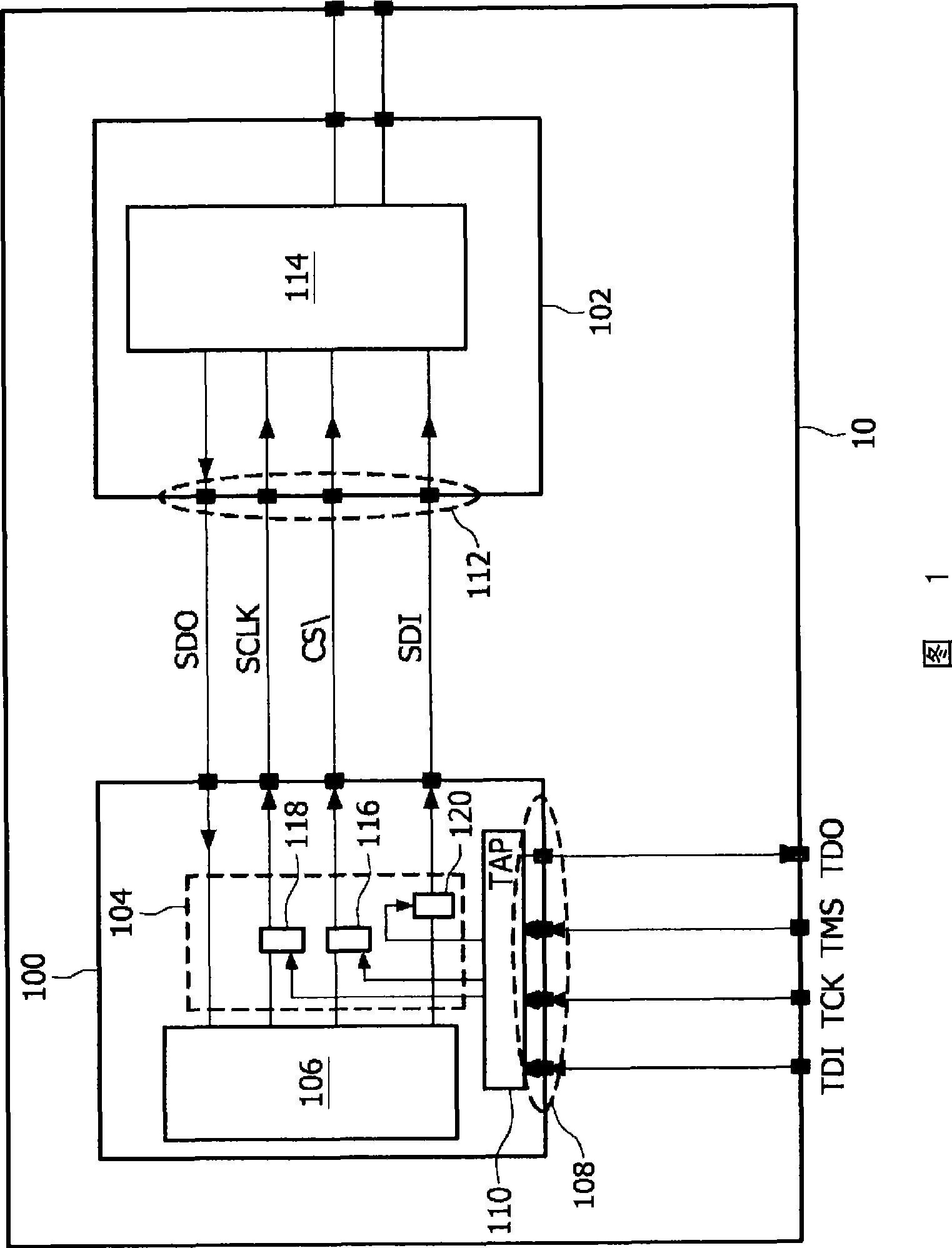
[0028] Referring to FIG. 1 , an integrated circuit 10 includes a first circuit portion 100 , a second circuit portion 102 , and a test access control (TAC) circuit 104 . The test access control circuit is shown schematically as part of the first circuit part, but it could of course be a separate circuit.

[0029] First circuit portion 100 includes digital core logic 106 , JTAG interface 108 and test access port (TAP) 110 . The JTAG interface 108 is a four / five-pin interface between the first circuit part 100 and the external pins of the integrated circuit 10, and is provided by each chip supporting the JTAG standard. According to the JTAG standard, JTAG interface 108 supports the following dedicated signals: Test Data In (TDI); Test Data Out (TDO); Test Clock (TCK); Test Mode Select (TMS);

[0030] "Test Reset" is an optional asynchronous reset signal and is not included in JTAG interface 108 of FIG. 1 . Although "test reset" is not shown in the embodiment of FIG. 1, the tes...


PUM


Abstract

An integrated circuit comprises a first circuit portion (106) with a JTAG interface (108) and a test access port (110). A second circuit portion (114) has a serial bus interface (112); and a test access control circuit (104) is connected to the JTAG interface (108) via the test access port (110). The first circuit portion (106) is connected to the serial bus interface (112) via the test access control circuit (104) and the test access control circuit (104) is programmable to be in a transparent mode or a test mode in response to a test mode select (TMS) signal from the JTAG interface (108). Thus, there is provided generic access to hidden serial bus interfaces while also maintaining speed performance such that the circuit portion/device under test can still be operated at device specification.

Description

technical field [0001] The present invention relates to the field of integrated circuits, and in particular to system-in-package (SIP) integrated circuits having internal circuitry with which it is desired to communicate via a serial bus interface. Background technique [0002] In modern system-in-package (SIP) integrated circuits (ICs), different chips are combined in one package to build a complete system. Communication between the digital chip contained in this SIP and the mixed-signal / radio frequency (RF) chip can be easily achieved using common serial bus interfaces (SPI, 3-WIRE, uWIRE). It is also known to use this serial bus at the chip level for controlling and debugging certain mixed-signal / RF chips. [0003] However, when such a serial bus is embedded in a SIP, the serial bus interface becomes inaccessible once the SIP is manufactured. Therefore, system testing, debugging and characterization of the mixed-signal / RF section are all severely hampered. [0004] In ...

Claims


Application Information

Patent Timeline
IPC IPC(8): G01R31/3185
CPCG01R31/318572
Inventor L·范德洛格特
Owner KONINKLIJKE PHILIPS ELECTRONICS NV
Why Eureka
Try Eureka