Exposure device and rectification device of baseal plate

An exposure device and substrate technology, which is applied in the direction of photolithography exposure device, overflow exposure, microlithography exposure equipment, etc., can solve the problems of incomplete adsorption, suction leakage, deformed substrate, etc., and achieve high-efficiency exposure and realization The effect of miniaturization

Active Publication Date: 2009-04-29
ADTEC ENG
View PDF0 Cites 5 Cited by
  • Summary
  • Abstract
  • Description
  • Claims
  • Application Information

AI Technical Summary

Problems solved by technology

[0004] However, compared with semiconductor wafers, substrates for printed wiring are prone to substrate deformation such as warpage and deformation, and the amount of deformation is also large, resulting in a gap between the substrate and the exposure stage, resulting in suction. Leakage, incomplete or difficult adsorption

Method used


Image

  • Exposure device and rectification device of baseal plate
  • Exposure device and rectification device of baseal plate
  • Exposure device and rectification device of baseal plate

Examples


Embodiment Construction

[0016] Embodiments of the exposure apparatus for printed wiring boards of the present invention will be described below with reference to the drawings.

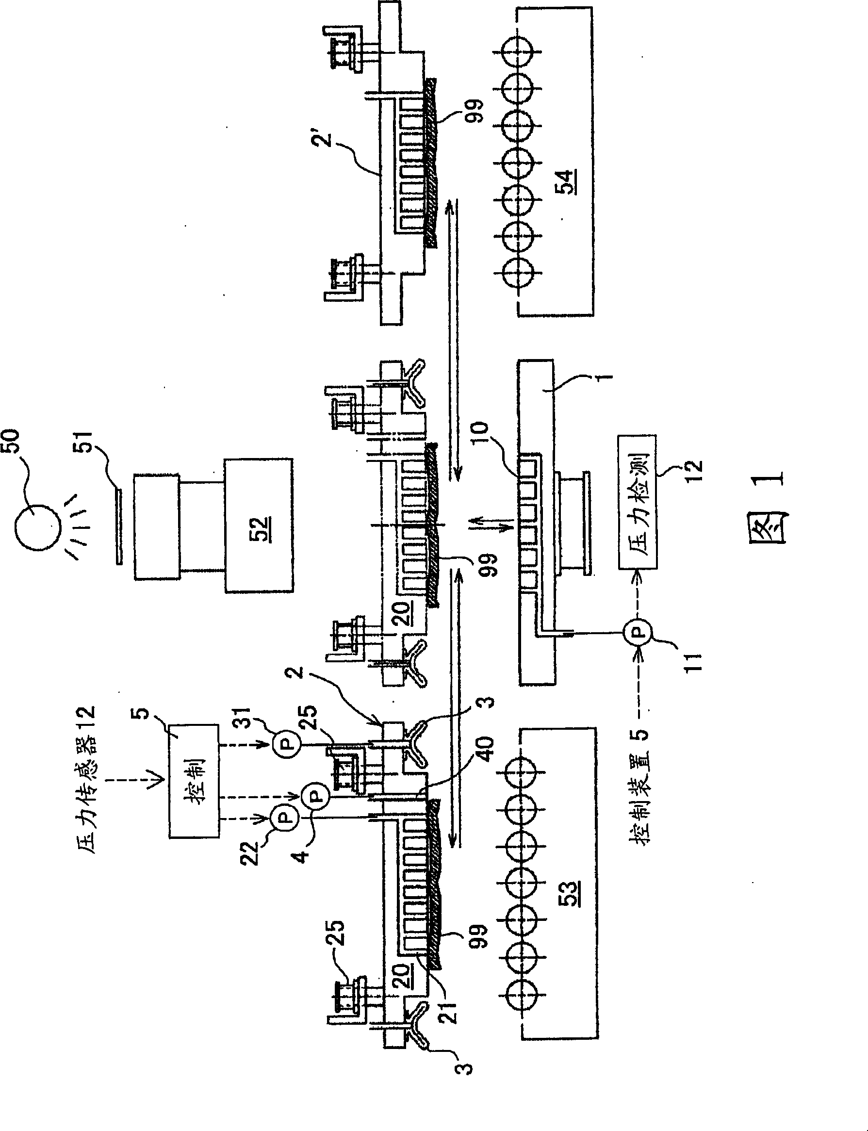
[0017] In FIG. 1 , an exposure stage 1 places a substrate 99 for printed wiring as an exposure target to be exposed, and exposes the substrate 99 through a light source 50 , a mask 51 , and a projection lens 52 . The exposure stage 1 is movable in the XYZ directions and rotatable in the θ direction by a driving device (not shown).

[0018] The exposure stage 1 is provided with a suction hole 10 , and the substrate 99 is suctioned and fixed by a suction pump 11 . A pressure sensor 12 is provided on the suction pump 11 to detect the suction pressure and detect whether the suction is performed normally.

[0019] On the entry side of the exposure stage 1 is provided a transfer device 2 configured to place the substrate 99 transferred from the previous process by the carry-in conveyor 53 on the exposure stage 1 .

[0020] The co...


PUM


Abstract

The invention provides an exposure device and a correction device of a base plate, characterized in that the exposure device may correct the base plate. A sealing piece (3) is exerted with positive pressure to stretch such that it is contacted with an exposure worktable (1) so as to generate a sealed space (90); the sealed space (90) is sucked by a vacuum sucking hole (40) and a vacuum pump (4); a plate (20) is pressed by atmospheric pressure; a base plate (99) is exerted with loads by the plate (20) and the exposure worktable (1) so as to correct the base plate (99). The vacuum pump (4) is stopped, the sealing piece (3) is shrank, a handling device (2) is withdrawn to a carrying-in conveyer (53), and exposure is them executed if the base plate of a sucking pump (11) is provided with an adsorptive pressure reaching a predetermined set value.

Description

technical field [0001] The present invention relates to an exposure device and a correction device for a substrate. Background technique [0002] In an exposure apparatus for manufacturing a printed circuit board, a structure is adopted in which a substrate conveyed by a substrate conveyance device is mounted and suction-fixed on an exposure stage for positioning to perform exposure. [0003] Patent Document 1: Japanese Patent Laid-Open No. 2005-370037 [0004] However, compared with semiconductor wafers, substrates for printed wiring are prone to substrate deformation such as warpage and deformation, and the amount of deformation is also large, resulting in a gap between the substrate and the exposure stage, resulting in suction. Leakage, there is the problem of incomplete or difficult adsorption. Contents of the invention [0005] The object of the present invention is to solve the above-mentioned problems of the prior art. [0006] In order to achieve the above objec...

Claims


Application Information

Patent Timeline
Patent Type & Authority Applications(China)
IPC IPC(8): G03F7/20H05K3/00
CPCG03F7/20H01L21/683H05K3/0023H05K3/22H05K2203/0508
Inventor 原贵之
Owner ADTEC ENG
Why Eureka
Try Eureka