Semiconductor packaging stack combination construction with movable outer terminal

A packaging stacking and combined structure technology, applied in semiconductor devices, semiconductor/solid-state device components, electric solid-state devices, etc., can solve problems such as solder joint fracture, and achieve the effect of increasing interface heat conduction, heat dissipation and temperature uniformity

Inactive Publication Date: 2010-06-02
POWERTECH TECHNOLOGY INC
View PDF8 Cites 0 Cited by
  • Summary
  • Abstract
  • Description
  • Claims
  • Application Information

AI Technical Summary

Problems solved by technology

Therefore, part of the solder joints of these second pins 123 bear excessive concentrated stress, especially the side edge pins of these second pins 123, there will be a problem of solder joint breakage

Method used


Image

  • Semiconductor packaging stack combination construction with movable outer terminal
  • Semiconductor packaging stack combination construction with movable outer terminal
  • Semiconductor packaging stack combination construction with movable outer terminal

Examples


Embodiment Construction

[0070] In order to further explain the technical means and effects of the present invention to achieve the intended purpose of the invention, the following is a detailed description of the specific implementation, structure, features and the semiconductor package stack assembly structure proposed by the present invention with reference to the accompanying drawings and preferred embodiments. Efficacy, as detailed below.

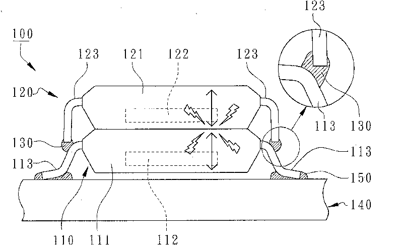
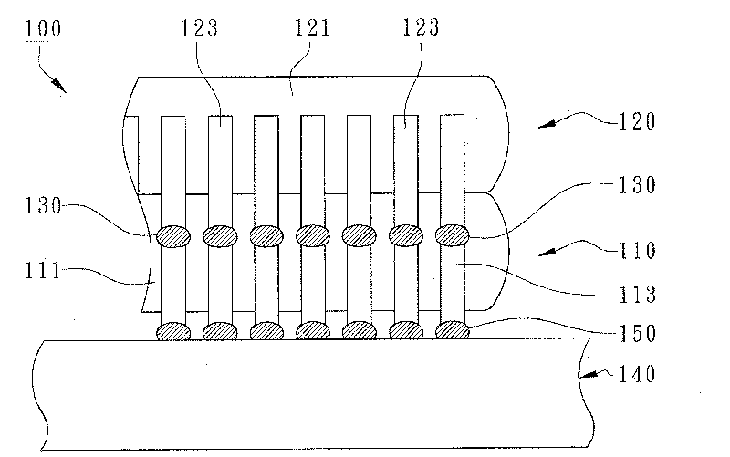
[0071] image 3 versus Figure 4 It is a semiconductor package stack assembly structure with movable external terminals disclosed in the first embodiment of the present invention. One specific package type can be TSOP (Thin Small Outline Package), but it can also be applied to TSOP and fine pitch ball grid array package (FBGA) with a chip on a socket.

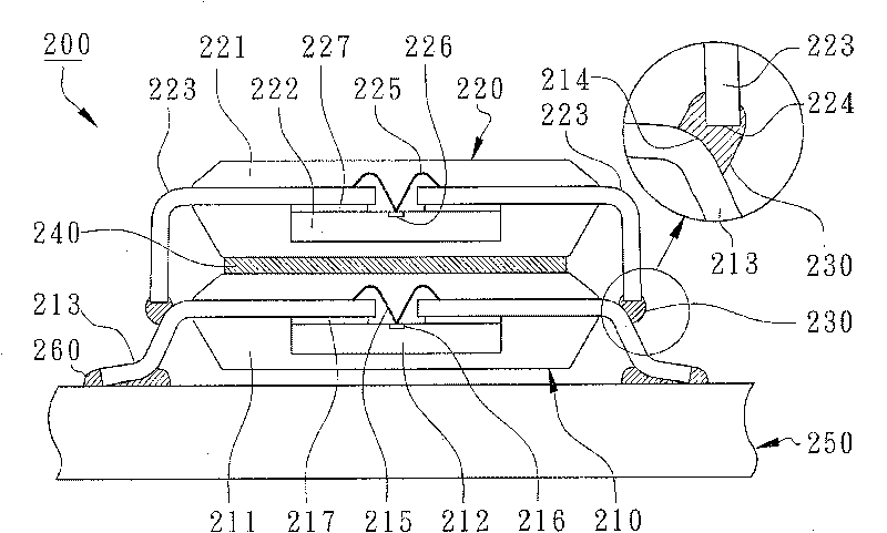
[0072] A semiconductor package stack assembly structure 200 with movable external terminals mainly includes a first semiconductor package 210, at least one second semiconductor package 220, and a soldering substance...


PUM


Abstract

The invention relates to a semiconductor sealing and stacking combination structure with movable external terminals, which mainly comprises a plurality of semiconductor sealing parts which are mutually stacked and a plurality of electrical connection components such as welding fluid so as to connect the external terminals of the semiconductor sealing parts such as outer leads of a lead frame. Eachsemiconductor sealing part seals at least one wafer by a sealing body, and the sealing body can move toward these electrical connection components so as to absorb stress among the semiconductor sealing parts. A stress relief layer can be formed among the semiconductor sealing parts in one embodiment.

Description

Technical field [0001] The present invention relates to a semiconductor package stack combination structure (POP device), and more particularly to a semiconductor package stack combination structure with movable external terminals. Background technique [0002] In recent years, high-tech electronic products have continuously introduced more user-friendly and better-function electronic products, resulting in the trend of lighter, thinner, shorter and smaller products. Therefore, a type of semiconductor device assembly is a vertical 3D stack of multiple semiconductor packages to meet the requirements of small surface bonding area and high-density device placement, which is called a POP device. Among them, the stackable semiconductor package component uses the lead frame as the chip carrier, and the cost is the lowest. It is welded and stacked to connect the external pins of the component (encapsulation body) to achieve the circuit series connection, but the external pins The solde...

Claims


Application Information

Patent Timeline
Patent Type & Authority Patents(China)
IPC IPC(8): H01L25/00H01L23/488H01L23/31
CPCH01L2224/32225H01L2224/32245H01L2224/48091H01L2224/4824H01L2224/4826H01L2224/73215H01L2924/15311
Inventor 范文正
Owner POWERTECH TECHNOLOGY INC
Why Eureka
Try Eureka