Semiconductor measuring probe bench with rotatable probe card

A technology for measuring probes and probe cards, which is used in semiconductor/solid-state device testing/measurement, measuring electricity, measuring devices, etc. Accuracy, effect of small test error

Inactive Publication Date: 2012-03-21
HEJIAN TECH SUZHOU
View PDF0 Cites 0 Cited by
  • Summary
  • Abstract
  • Description
  • Claims
  • Application Information

AI Technical Summary

Problems solved by technology

like figure 2 As shown, since the test key 9 usually has two placement directions along the horizontal and vertical directions, when the measurement direction needs to be converted, two methods are mainly used for detection: method one, the wafer carrier 5 itself can be rotated 90 degrees, but the disadvantage The rotation of the crystal plate 5 causes the positioning accuracy to decrease. Assume that the motion error of the crystal plate along the horizontal track 2 is A, the motion error of the crystal plate along the vertical track 3 is B, and the motion error of the crystal plate along the upper and lower tracks 4 is C. The rotation error of the crystal disk 5 itself is D, and the total error of the movement of the crystal disk relative to the probe card reaches A*B*C*D. With the progress of the semiconductor manufacturing process, the test key 9 is getting smaller and smaller, and the accuracy required for the measurement is getting higher and higher. The higher the value, the greater the measurement error will be, and the measurement accuracy will be reduced; in the second way, the wafer is transferred from the wafer carrier 5 to an external rotary machine (not shown in the figure), and then moved back to the carrier after turning 90 degrees. Crystal disk 5, the total error of the movement of the crystal disk relative to the probe card is A * B * C, but the disadvantage is that this method requires an external machine, and it will take more time to transfer the wafer back and forth

Method used


Image

  • Semiconductor measuring probe bench with rotatable probe card
  • Semiconductor measuring probe bench with rotatable probe card
  • Semiconductor measuring probe bench with rotatable probe card

Examples


Embodiment Construction

[0017] The semiconductor measuring probe station of the rotatable probe card according to the present invention will be further described in detail below in conjunction with the accompanying drawings and specific embodiments.

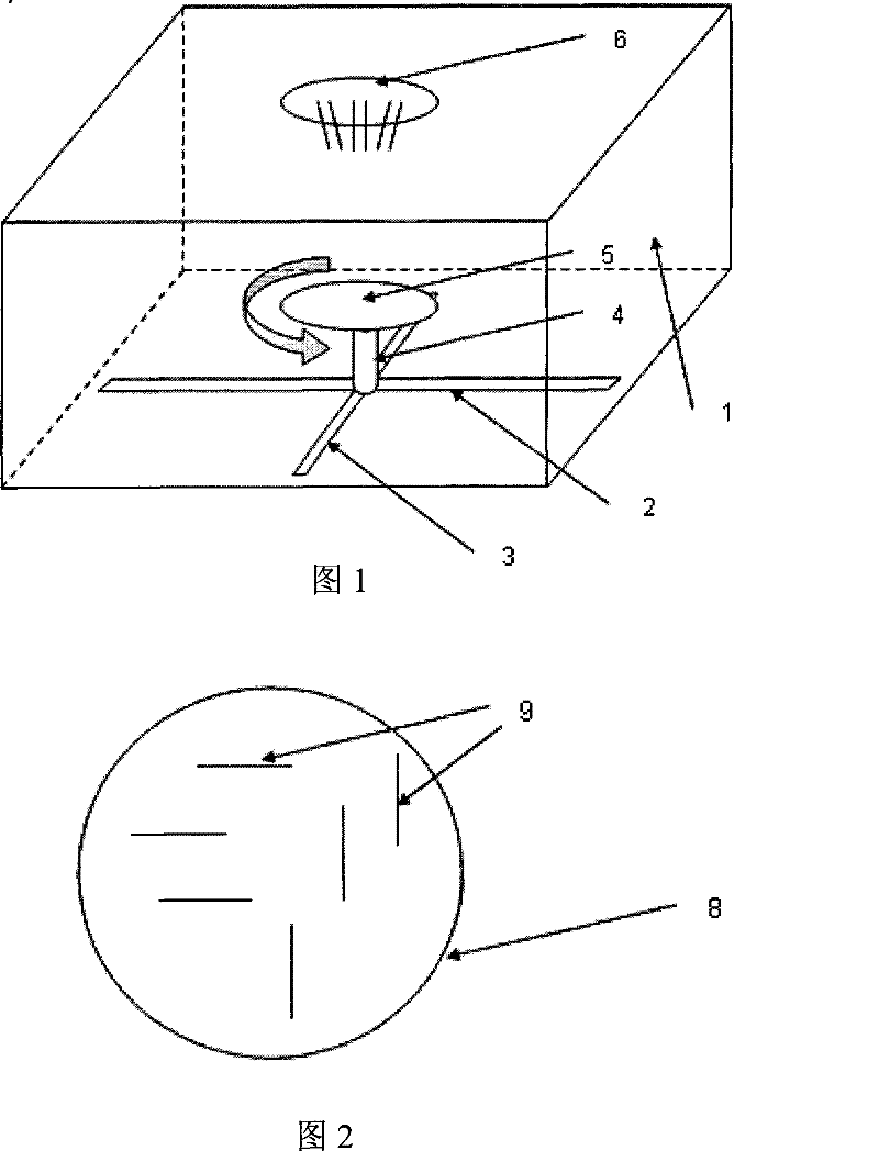
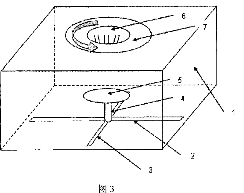
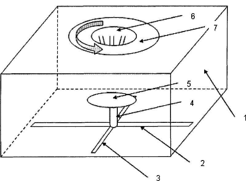
[0018] In the semiconductor manufacturing process, component parameter measurement is a very important monitoring step. By measuring the electrical parameters of components such as resistors, capacitors, and transistors in the test key 9 of the wafer 8, the characteristics of the components and problems on the production line can be reflected.

[0019] The present invention improves the traditional method, adopts the concept of relative motion, does not rotate the wafer carrier 5, but rotates the probe card 6 to measure the wafer. First, a controllable rotating device 7 is arranged on the main body top plane of the probe station 1, so that the probe card mounted on it is opposite to the wafer carrier below, and the rotating device 7 is controlled by the ...


PUM


Abstract

The invention provides a semiconductor measurement probe station with a rotatable probe card, which at least comprises a probe station main-body, an orbit and a wafer bearing disc; the orbit is positioned under the probe station main-body, and used for bearing and moving the wafer bearing disc; and the wafer bearing disc is positioned on the orbit and is used for holding a wafer, wherein, a swiveling mechanism positioned above the wafer bearing disc and used for installing the probe card is also included. The semiconductor measurement probe station adopts the relative movement conception, installs a traditional immobilized probe card to a rotating device, increases the rotary measuring accuracy greatly, and cannot waste more time.

Description

technical field [0001] The invention relates to a semiconductor measurement probe station, in particular to a semiconductor measurement probe station with a rotatable probe card. Background technique [0002] In the semiconductor manufacturing process, component parameter measurement is an important monitoring step. By measuring the electrical parameters of components such as resistance, capacitance, and transistors in the test key on the wafer, it can reflect component characteristics and problems on the production line. During the measurement, the wafer is carried on the wafer carrier in the semiconductor measurement probe station, and after contacting with the probe card, the measurement signal is applied to the test key through the probes on the probe card. The structure of the traditional probe station is as follows figure 1 As shown, it includes a probe station 1 , a horizontal track 2 , a vertical track 3 , an upper and lower track 4 , a wafer carrier 5 and a probe c...

Claims


Application Information

Patent Timeline
Patent Type & Authority Patents(China)
IPC IPC(8): G01R1/02G01R1/073H01L21/66
Inventor 宋丰王政烈
Owner HEJIAN TECH SUZHOU
Why Eureka
Try Eureka