Condenser type touch screen
A capacitive touch screen and electrode technology, which is applied to the input/output process of electrical digital data processing, instruments, and data processing, etc. Display the effect of visual effects
- Summary
- Abstract
- Description
- Claims
- Application Information
AI Technical Summary
Problems solved by technology
Method used
Image
Examples
Embodiment 1
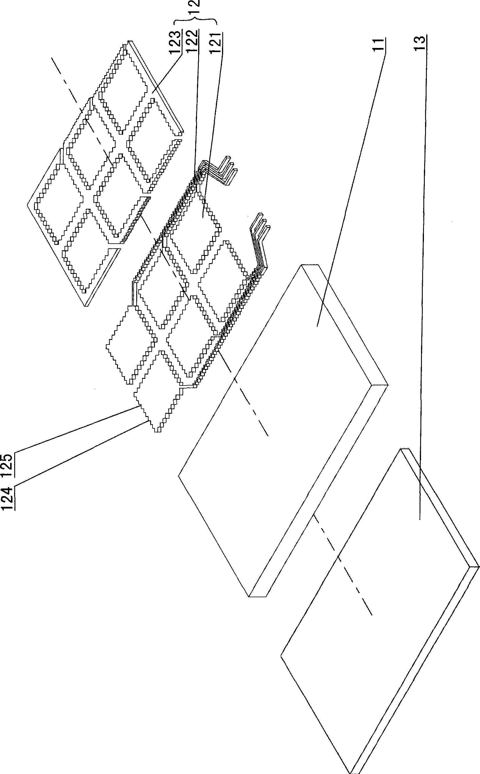
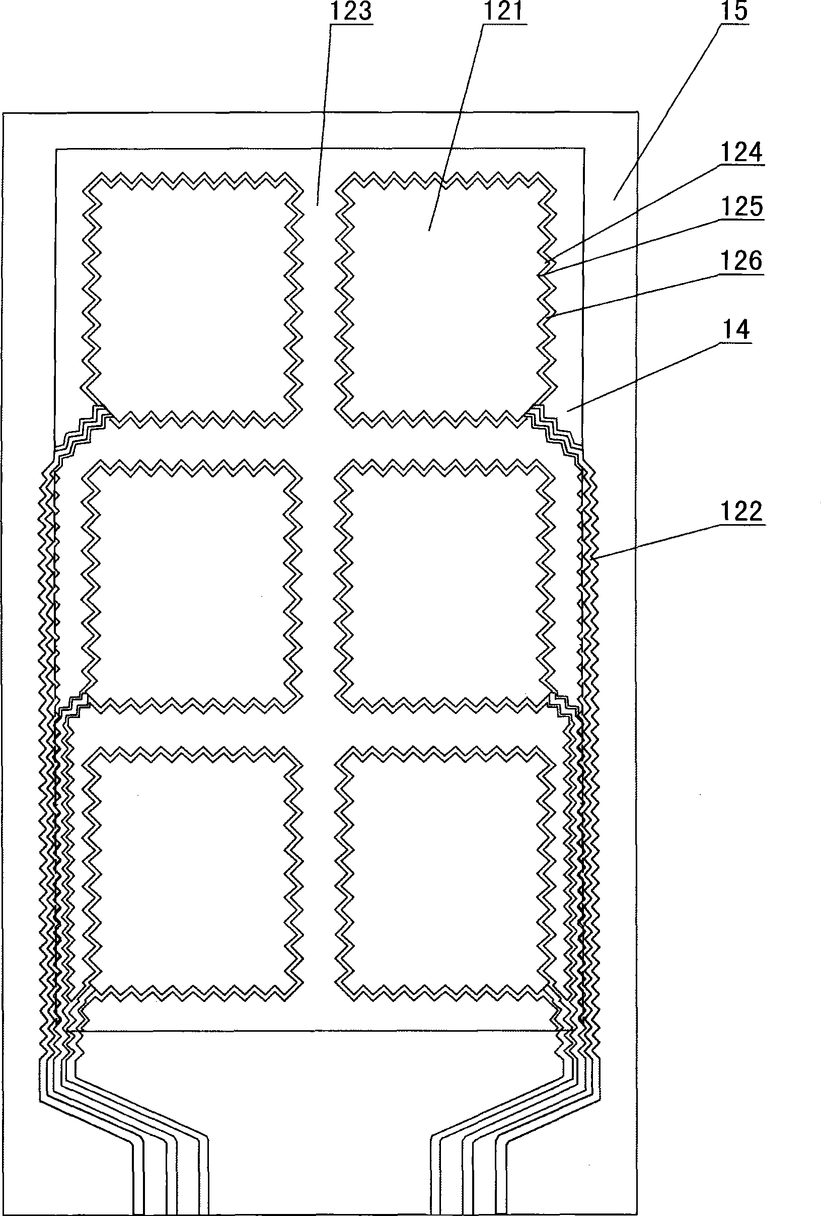
[0026] like figure 1 and figure 2 As shown, this capacitive touch screen includes a transparent insulating layer 11, a transparent electrode conductive layer 12 and a shielding layer 13, the transparent electrode conductive layer 12 is arranged on the outer surface of the transparent insulating layer 11, and the shielding layer 13 is arranged on the transparent insulating layer 13 On the inner side of the layer 11 (when the capacitive touch screen is configured on the display device, the shielding layer 13 is on the side of the capacitive touch screen close to the display device, that is, the shielding layer 13 is located between the transparent insulating layer 11 and the display device), the transparent electrode is conductive Layer 12 is composed of a plurality of electrodes (including six sensing electrodes 121 , six lead electrodes 122 and filling electrodes 123 ). This capacitive touch screen can be used for single-touch operation. In addition, the number of sensing e...
Embodiment 2
[0039] like Image 6 and Figure 7 As shown, the capacitive touch screen includes a first transparent insulating layer 21, The first transparent electrode conductive layer 22 , the insulating separation layer 23 , the second transparent electrode conductive layer 24 , the second transparent insulating layer 25 and the shielding layer 26 . The first transparent electrode conductive layer 22 is arranged on the inner side of the first transparent insulating layer 21, and the second transparent electrode conductive layer 24 is arranged on the outer side of the second transparent insulating layer 25; the insulating spacer layer 23 is made of insulating material, so that the first There is no conduction between the first transparent electrode conductive layer 22 and the second transparent electrode conductive layer 23 ; the shielding layer 26 is disposed on the inner side of the second transparent insulating layer 25 .
[0040] The first transparent electrode conductive layer 22 i...
PUM
| Property | Measurement | Unit |
|---|---|---|
| Top angle | aaaaa | aaaaa |
Abstract
Description
Claims
Application Information


