
OPC method for mask preparation course in semiconductor manufacturing process

A semiconductor and process technology, applied in the field of optical approximation correction, can solve problems such as difficulty in obtaining images and smaller process windows, and achieve the effects of improving mutual conflicts, expanding process windows, and avoiding possibilities

Active Publication Date: 2009-08-05
SEMICON MFG INT (SHANGHAI) CORP
View PDF1 Cites 15 Cited by
  • Summary
  • Abstract
  • Description
  • Claims
  • Application Information

AI Technical Summary

Problems solved by technology

Then, if most of the information of a pattern is contained in its high-frequency part, it is relatively more difficult to obtain a satisfactory image of such a pattern with current imaging equipment, so for isolated patterns, the process window must become smaller
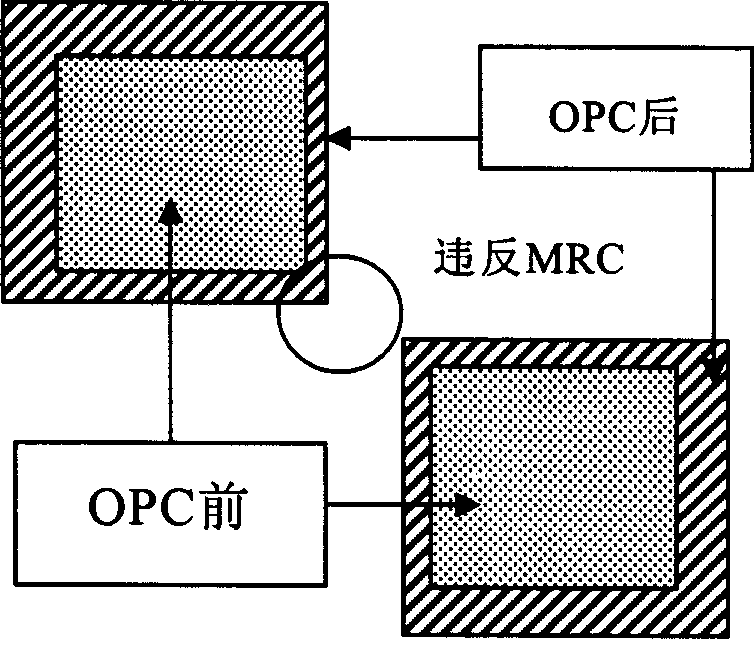
[0013] The problems encountered by the existing OPC technology mentioned above not only appear in the OPC of the pattern of the connection hole layer, but also encounter the same problem for those rectangular patterns that are similar to squares.

Method used


Image

  • OPC method for mask preparation course in semiconductor manufacturing process
  • OPC method for mask preparation course in semiconductor manufacturing process
  • OPC method for mask preparation course in semiconductor manufacturing process

Examples


Embodiment 1

[0045] Before prior art OPC for square via pattern, as in Figure 4 As shown, the shape of the square connecting hole is changed into an octagon with eight sides of a to h, the length of the truncated side is controlled to be 1 / 4 of the side length of the square pattern, and the internal angles of the octagon are 135°. The octagon is then targeted for prior art OPC. After the OPC is done, the pattern obtained is exposed to the wafer to obtain an approximate circle, which is inscribed with the octagon before OPC in the prior art. The advantages of the present invention are explained below by describing the process of performing OPC of the prior art on the octagon.

[0046] First of all, through this solution, the existing OPC oscillation and convergence problems are improved.

[0047] After the square connection hole is changed to an octagon, the steps of OPC in the prior art are carried out with the octagon as the target. Figure 5 As shown in the figure, arrows are used t...

Embodiment 2

[0063] Such as Figure 12 As shown, the shape of the square connection hole is modified to an equilateral 16-sided shape, where the 16-sided shape has four vertices located at the midpoints of the four sides of the original square. The 16-gon is then targeted for state-of-the-art OPC. In this way, an approximate circle is obtained when exposed to the wafer, and the approximate circle is inscribed with the 16-gon before OPC.

[0064] This modification greatly improves the OPC that only uses the prior art, and the principle is the same as that of the first embodiment. The experimental data of improving the process window of the regular polygon and the hexagonal connecting hole is given here. As shown in Table 2, for different lithographic focal depths, the 16-gon is within the allowable error requirement within a larger lithographic focal depth range relative to the square, that is, the 16-gon has better process window.

[0065] Table 2

[0066] Photolithography f...


PUM


Abstract

The present invention provides a method for optical proximity correction (OPC), which can greatly prevent the problems appearing previously in optical proximity correction. The scheme provided by the present invention alters the shape of layout patterns before the existing optical proximity correction, generates other convex polygon patterns on the basis of existing layout patterns, and then conducts optical proximity correction with the convex polygon patterns as the target.

Description

technical field [0001] The present invention relates to the photolithography process in the semiconductor manufacturing industry, and in particular to the optical proximity correction (Optical Proximity Correction, abbreviated as OPC, the abbreviation OPC is used to refer to the optical proximity correction) method in the process of preparing the mask. Background technique [0002] Integrated circuit manufacturing technology is a complex process that is updated every 18 to 24 months. A key parameter that characterizes integrated circuit manufacturing technology, the minimum feature size is the critical dimension (Critical Dimension), from the initial 125 microns (10 -6 m) to the current 0.13 microns or even smaller. This makes it possible to have millions of components per chip. [0003] Photolithography is the driving force behind the development of integrated circuit manufacturing processes, and it is also one of the most complex technologies. Compared with other indivi...

Claims


Application Information

Patent Timeline
IPC IPC(8): G03F1/14G03F1/36
Inventor 刘庆炜
Owner SEMICON MFG INT (SHANGHAI) CORP
Learn More