Check patentability & draft patents in minutes with Patsnap Eureka AI!

Resistive memory device and method of fabricating the same

A resistive memory and device technology, applied in static memory, digital memory information, electrical components, etc., can solve the problems of irregular oxygen vacancy filaments, uneven characteristic distribution, and the inability of resistive memory devices to present uniform characteristic distribution, etc.

Inactive Publication Date: 2010-01-27
SK HYNIX INC
View PDF1 Cites 17 Cited by
  • Summary
  • Abstract
  • Description
  • Claims
  • Application Information

AI Technical Summary

Problems solved by technology

[0008] However, due to the irregular generation of oxygen vacancy filaments, the resistive memory device cannot exhibit uniform characteristic distribution, such as voltage / current distribution in set / reset mode
This problem of non-uniform characteristic distribution becomes more serious as resistive memory devices are miniaturized

Method used


Image

  • Resistive memory device and method of fabricating the same
  • Resistive memory device and method of fabricating the same
  • Resistive memory device and method of fabricating the same

Examples


Embodiment Construction

[0014] In the drawings, the dimensions of layers and regions are particularly exaggerated for clarity of illustration. It will also be understood that when a layer (or film) is referred to as being 'on' another layer or substrate, it can be directly on the other layer or substrate, or intervening layers may also be present. Further, it will be understood that when a layer is referred to as being 'under' another layer, it can be directly under, but one or more intervening layers may also be present. In addition, it will also be understood that when a layer is referred to as being 'between' two layers, it can be the only layer between the two layers, or one or more intervening layers may also be present. Like reference numerals refer to like devices throughout the drawings.

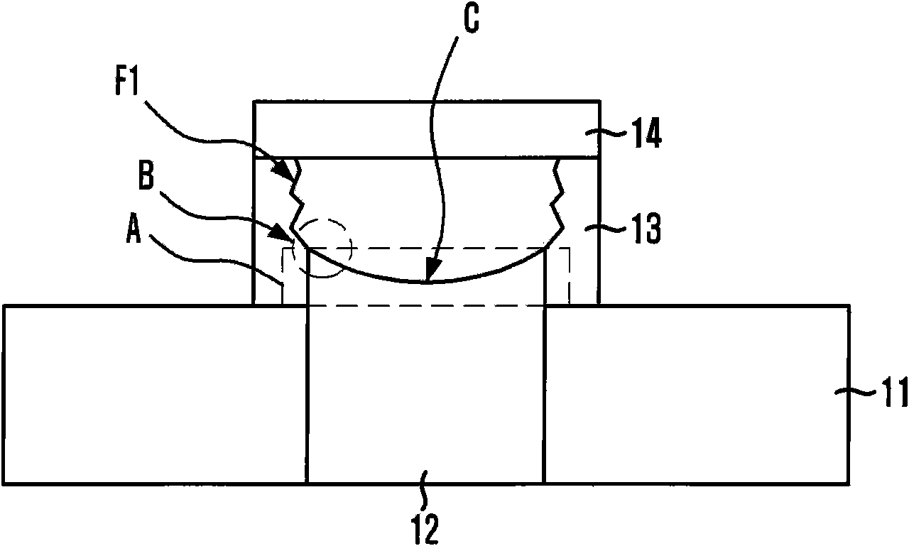
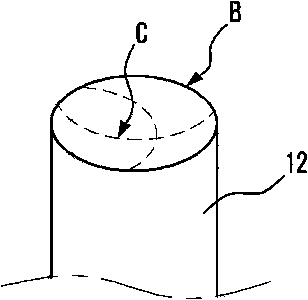
[0015] Figure 1A and 1B They are respectively a cross-sectional view and a partial perspective view of a resistive memory device according to an embodiment. Particularly, Figure 1A and 1B A resistive ...


PUM


Abstract

A resistive memory device includes: a substrate, an insulation layer arranged over the substrate, a first electrode plug penetrating the insulation layer from the substrate, having a portion protruded out of an upper portion of the insulation layer, and having peaks at edges of the protruded portion, a resistive layer disposed over the insulation layer and covering the first electrode plug, and a second electrode arranged over the resistive layer.

Description

[0001] This application claims the benefit of Korean Patent Application No. 10-2008-0072477 filed on July 24, 2008, the entire contents of which are hereby incorporated by reference. technical field [0002] The present invention relates to a semiconductor device manufacturing technology, in particular to a resistive memory device utilizing impedance change such as a nonvolatile resistive random access memory (ReRAM) and a manufacturing method thereof. Background technique [0003] Recently, developers have been developing next-generation memory devices that can replace dynamic random access memory (DRAM) and flash memory. [0004] One of the next-generation memory devices is a resistive memory device, which takes advantage of the characteristics of a resistive layer that can switch between at least two different impedance states by drastically changing the resistance value in response to a bias voltage applied to the resistive layer. to switch between. [0005] The structu...

Claims


Application Information

Patent Timeline
IPC IPC(8): H01L45/00G11C11/56
CPCH01L45/147H01L45/1675H01L45/1273H01L45/146H01L45/145H01L45/08H01L45/1233H10N70/24H10N70/8418H10N70/826H10N70/8833H10N70/883H10N70/8836H10N70/011H10N70/063H01L21/02107
Inventor 郑璲钰
Owner SK HYNIX INC
Features
  • R&D
  • Intellectual Property
  • Life Sciences
  • Materials
  • Tech Scout
  • Unparalleled Data Quality
  • Higher Quality Content
  • 60% Fewer Hallucinations
Learn More