Pixel structure
A technology of pixel structure and dielectric layer, applied in optics, instruments, electrical components, etc., can solve the problem that the display effect of wide viewing angle cannot be effectively improved, achieve a good display effect of wide viewing angle, and improve the display effect
- Summary
- Abstract
- Description
- Claims
- Application Information
AI Technical Summary
Problems solved by technology
Method used
Image


Examples
Embodiment Construction
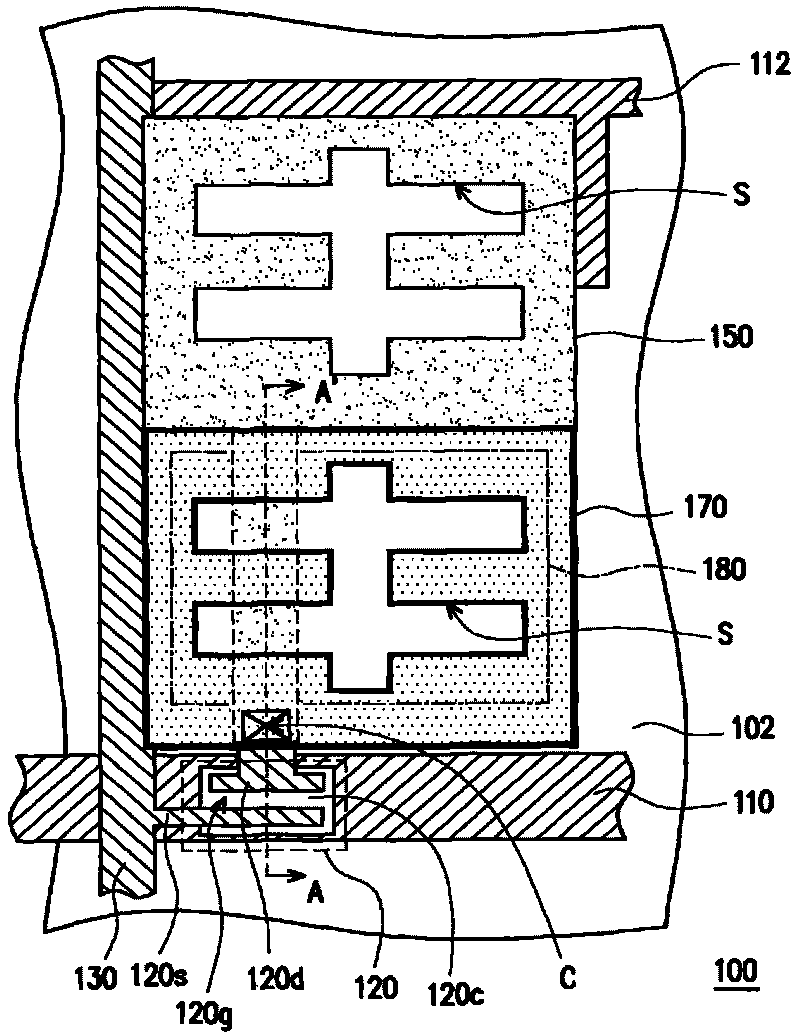
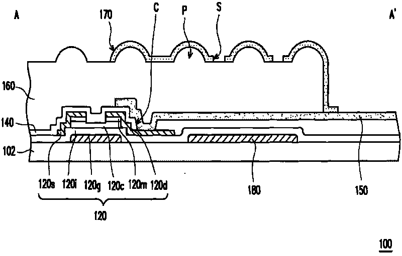
[0031] figure 1 is a top view of a pixel structure according to an embodiment of the present invention, and figure 2 is a cross-sectional view of a pixel structure according to an embodiment of the present invention. For simplicity of illustration, figure 1 The drawing of the first dielectric layer, the second dielectric layer and the third dielectric layer is omitted in the figure, but these film layers can be clearly seen in figure 2 middle. Please also refer to figure 1 and figure 2 , The pixel structure 100 of the present invention includes a substrate 102, a scanning line 110, an active component 120, a data line 130, a second dielectric layer 140, a penetrating electrode 150, a third dielectric layer 160, a The reflective electrode 170 and a light shielding layer 180 .
[0032] like figure 2 As shown, the active device 120 on the substrate 102 may include a gate 120g, a first dielectric layer 120i, a channel layer 120c, an Ohmic contact layer 120m, a source 12...
PUM
 Abstract
Description
Claims
Application Information
 - R&D
- Intellectual Property
- Life Sciences
- Materials
- Tech Scout
- Unparalleled Data Quality
- Higher Quality Content
- 60% Fewer Hallucinations
Browse by: Latest US Patents, China's latest patents, Technical Efficacy Thesaurus, Application Domain, Technology Topic, Popular Technical Reports.
© 2025 PatSnap. All rights reserved.Legal|Privacy policy|Modern Slavery Act Transparency Statement|Sitemap|About US| Contact US: help@patsnap.com