Loading table structure and processing device

A mounting table and structure technology, applied in semiconductor/solid-state device manufacturing, electrical components, circuits, etc., can solve problems such as increased operating costs, leakage of purge gas, and difficult process execution

Inactive Publication Date: 2010-07-07
TOKYO ELECTRON LTD
View PDF6 Cites 18 Cited by
  • Summary
  • Abstract
  • Description
  • Claims
  • Application Information

AI Technical Summary

Problems solved by technology

[0019] However, at this time, it is difficult to prevent the purge gas supplied into the column 4 from leaking to the processing space side in the processing container through the above-mentioned minute gap.
As a result, it is difficult to perform processes under high vacuum
In addition, there is also a problem of high operating costs due to the large consumption of purge gas

Method used


Image

  • Loading table structure and processing device
  • Loading table structure and processing device
  • Loading table structure and processing device

Examples


Embodiment approach

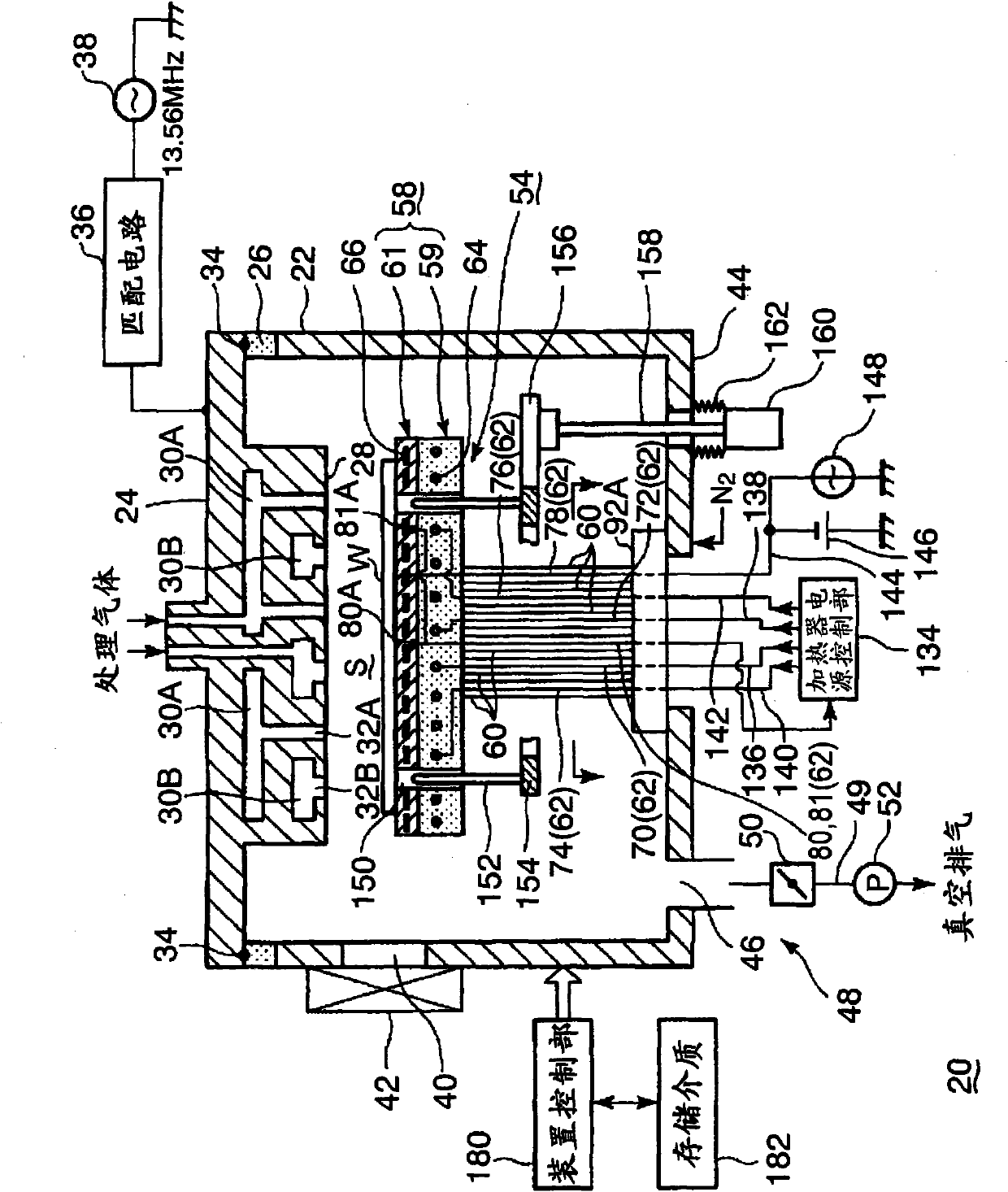
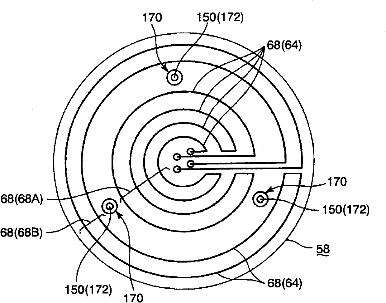
[0145]However, in each of the above-described embodiments, the process gas for film formation surrounds the back side of the mounting table 58 during film formation, and the processing gas enters the pin insertion holes 150 formed in the mounting table bolts 170 . Here, when the wafer W is placed on the stage 58, in order to suppress misalignment, the inner diameter of the pin insertion hole 150 is made, for example, about 4 mm, and the diameter of the push-up pin 152 is made, for example, about 3.8 mm to reduce the pin insertion size. The gap between the through hole 150 and the push pin 152 . Accordingly, when the processing gas for film formation enters the pin insertion hole 150 , the thin film accumulates little by little in the inside, which hinders the lifting operation of the lift pin 152 . Therefore, it is necessary to regularly or irregularly perform dry etching and wet etching to perform frequent cleaning operations, and in this case, there is a problem of lowering ...


PUM


Abstract

A loading table structure which is adapted, in order to prevent damage to the loading table, so that large thermal stress does not occur in the loading table and so that the amount of supply of a purge gas for corrosion prevention to the loading table is minimized. The loading table structure (54) is formed in a processing container (22) capable of discharging gas contained therein and is used to load thereon an object (W) to be processed. The loading table structure (54) is provided with a loading table (58) on which the object (W) to be processed is loaded and which consists of a dielectric, a heating means (64) which is provided to the loading table (58) and which heats the object (W) to be processed loaded on the loading table (58), and protective strut tubes (60) which are mounted so as to vertically rise from the bottom section (44) of the processing container (22), which have upper ends joined to the lower surface of the loading table (58) to support the loading table (58), and which consist of a dielectric. A functional bar (62) extending up to the loading table is inserted into each protective strut tube (60).

Description

technical field [0001] The present invention relates to a processing device and a stage structure for a target object such as a semiconductor wafer. Background technique [0002] In general, in the manufacture of semiconductor integrated circuits, various individual processes such as film formation, etching, heat treatment, modification, and crystallization are repeatedly performed on a target object such as a semiconductor wafer. The desired integrated circuit is thus formed. When performing the above-mentioned various treatments, the necessary processing gas is corresponding to the type of the treatment, such as film-forming gas or halogen gas during film-forming treatment, ozone gas during modification treatment, etc. N 2 Inert gas such as gas or O 2 Gas and the like are introduced into each processing container. [0003] For example, a sheet-type processing apparatus for heat-treating one semiconductor wafer includes, for example, a mounting table in which a resistan...

Claims


Application Information

Patent Timeline
Patent Type & Authority Applications(China)
IPC IPC(8): H01L21/683
CPCH01L21/68757H01L21/67069H01L21/67248H01L21/68792
Inventor 田中澄小松智仁川崎裕雄
Owner TOKYO ELECTRON LTD
Why Eureka
Try Eureka