
Full implanting board of printed circuit board and connecting method thereof

A technology for printed circuit boards and bonding methods, which is applied in the structural connection of printed circuits, printed circuit components, and printed circuit assembly of electrical components, and can solve the problems of large loss of material components, decreased utilization rate of SMT production lines, and defective sub-boards And other issues

Active Publication Date: 2012-06-27
D TEK TECHNOLOGY CO LTD
View PDF0 Cites 0 Cited by
  • Summary
  • Abstract
  • Description
  • Claims
  • Application Information

AI Technical Summary

Problems solved by technology

[0005] 1. As a result of the use of 0201 components and the high density of components, it is easy to lead to empty soldering and short circuits, and the cost of rework is very high
[0006] 2. If 01005 components are used, there is also the problem that the defects of empty welding and short circuit cannot be reworked, which makes the loss of material components very large
Due to the uneven expansion and contraction of the PCB, it will cause the cumulative error of the spacing between each PCB, and each PCB also has a different error (about 40 ~ 120μm), so if the 01005 component is used, the PCB manufacturer will be forced to use a single board Design (does not use parallel process), but the use of single-board PCB will cause a time bottleneck of 20 seconds in the cycle time of the printing machine in the SMT process, and the utilization rate of the production line worth NT$40 million will be lower than 50%. The utilization rate of the production line cannot be improved
[0009] 2. In order to take into account the SMT utilization rate, some manufacturers still combine PCBs into multi-connected boards, which will inevitably bear two additional risks. One is that the single steel plate of the printing machine cannot be corrected in time according to different PCB expansion and contraction sizes at any time, resulting in Solder paste printing offset component tombstoning and empty soldering problems; the second is that there will be defective boards with broken inner edge lines and short circuits in the multi-connected boards, which will become another factor that leads to a decrease in the utilization rate of the SMT production line. Or because the SMT factory rejects the multi-connection board, the purchase cost will increase significantly
[0010] 3. Due to the relationship between the touch screen, the layout design of this type of PCB components is bound to arrange a large number of components on the back of the non-touch surface. This will cause a very large ratio of the number of components on the front and back of the PCB, unless the PCB manufacturer can adopt positive , The back side is combined into a multi-connected board design (in fact, this kind of combined board design will cause the problem of lower pass rate and cumulative error), otherwise it will cause the problem that the utilization rate of the SMT production line will be greatly reduced
[0012] 1. In order to meet the consideration of the output of the SMT process, it is generally possible to combine multiple PCBs into one large board. However, due to the problem of short-circuiting of the inner layer of the sub-boards, there will be "explosion boards" due to multiple PCBs. It will reduce the production efficiency of SMT, so the expensive SMT manufacturing cost will generally be accommodated, and the PCB is required to scrap the combined board with defective sub-boards, so that the manufacturing cost of PCB will be greatly increased by more than 40% of the material cost
Or as shown in Annex 1 of the reference document of the prior art, the bad sub-board in the combined board must be replaced by a good board
[0013] 2. The expensive mobile phone HDI printed circuit board, because SMT needs a PCB board edge to facilitate delivery and transportation, so the cost of the PCB board edge material is relatively high. For a piece of 10×45mm mobile phone HDI, it accounts for about 10%. material and process costs
[0014] 3. In the past, due to the large passive components used in SMT, the spacing between the two sub-boards of the merged version was looser, but the HDI printed circuit boards for mobile phones are mainly 0201 or even 01005 components, so the merged board will be Due to the excessive cumulative error between two sub-boards, PCBs that are of good quality on the inner layer of the sub-boards are scrapped. This problem is the biggest challenge for PCB manufacturing costs in the future.

Method used


Image

  • Full implanting board of printed circuit board and connecting method thereof
  • Full implanting board of printed circuit board and connecting method thereof
  • Full implanting board of printed circuit board and connecting method thereof

Examples


Embodiment Construction

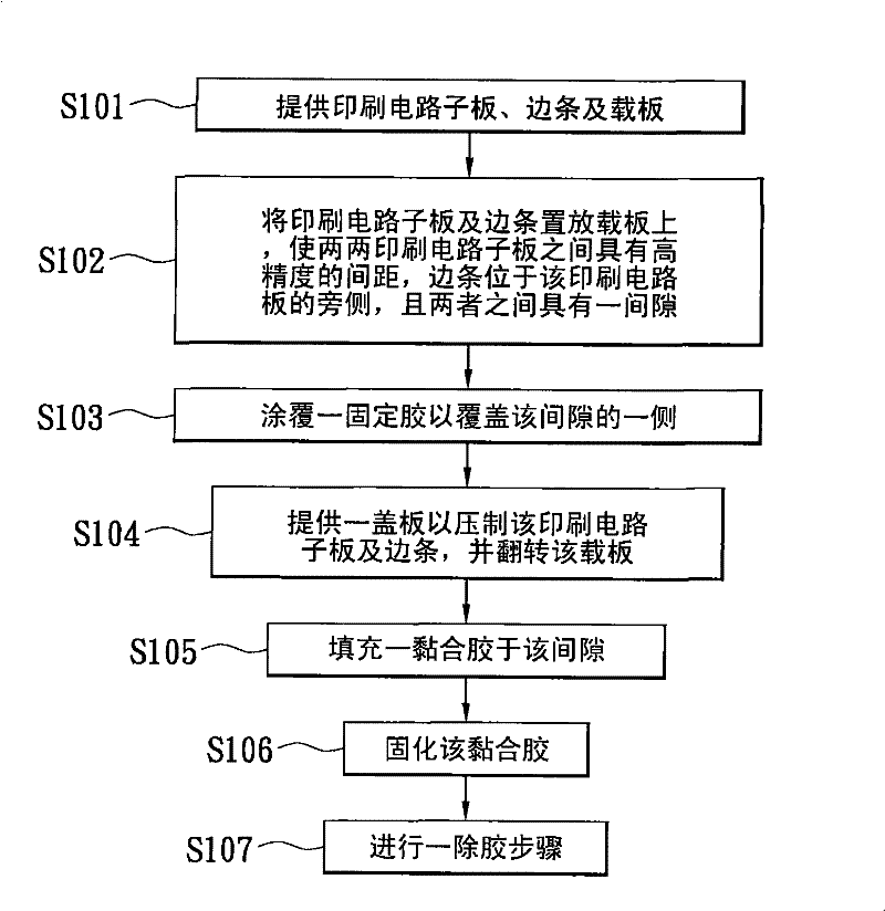
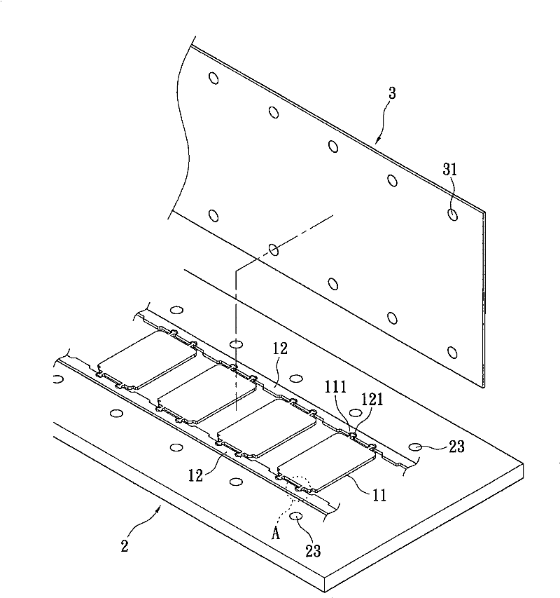
[0043] see figure 1 , the present invention provides a fully-planted printed circuit board and a bonding method thereof, the bonding method can carry out high-precision bonding of multiple printed circuit sub-boards and edge strips to form a fully-planted printed circuit board structure, The bonding method includes the following steps (see also Figure 2 to Figure 4A ):

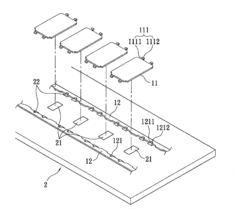
[0044] Step S101 : providing a plurality of printed circuit sub-boards 11 and at least two side strips 12 . In this embodiment, the present invention combines four printed circuit boards 11 with two edge strips 12 , but it is not limited thereto.

[0045] Step S102: Use the camera module to locate the plurality of printed circuit sub-boards 11 and at least two side strips 12 on a carrier board (see figure 2). In this step, the present invention utilizes two camera modules to respectively extract the upper surface image and the lower surface image of the printed circuit sub-board 11 (which may also includ...


PUM


Abstract

Thee invention provides a full implanting board of a printed circuit board and a connecting method thereof. The connecting method comprises the following steps of: providing a plurality of printed circuit sub-boards and at least two edges; providing at least two pickup modules which extract upper surface images and lower surface images of the printed circuit sub-boards respectively, and placing the plurality of printed circuit sub-boards and the two edges on a support plate by using the upper surface images and the lower surface images so that the adjacent two printed circuit sub-boards have high-precision distance and a clearance with a predetermined width is formed between the two printed circuit sub-boards and the two edges; coating a fixing glue on the printed circuit sub-boards and the two edges to cover the clearance; providing a cover plate on the support plate to press the printed circuit sub-boards and the two edges, and turning the support plate; filling adhesive in the clearance; performing a drying step to solidify the adhesive; and performing an adhesive removing step to remove the solidified non-solid adhesive. The method can solve the problem of accumulated error ofmultiple connecting boards.

Description

technical field [0001] The invention relates to a full planting board of a printed circuit board and a bonding method thereof, in particular to a method of bonding a printed circuit sub-board and side strips, so as to avoid the problem of accumulative errors in the process of miniaturized electronic components, and can be used at a lower unit price. Low side strips effectively reduce costs. Background technique [0002] With the advancement of the electronic application industry, the most noteworthy focus of mobile communication devices at present is the success of touch panel technology, and the application of mobile communication devices has successfully been pushed to another emerging market. World-renowned brands or R&D teams Both have successively announced to actively step into the R&D and production of this field. This market is a global high-tech competition. According to estimates, there is an annual demand of about 300 million products, and there is an increasing t...

Claims


Application Information

Patent Timeline
Patent Type & Authority Patents(China)
IPC IPC(8): H05K3/36H05K1/14
Inventor 费耀祺
Owner D TEK TECHNOLOGY CO LTD
Learn More