Image sensor and high-conversion-gain and low-noise pixel readout circuit

A technology of image sensor and readout circuit, which is applied in the direction of TV, electrical components, color TV, etc., and can solve the problems of not being suitable for high-density CMOS image sensors and occupying chip area.

Inactive Publication Date: 2013-03-13
HIMAX IMAGING LIMITED
View PDF0 Cites 0 Cited by
  • Summary
  • Abstract
  • Description
  • Claims
  • Application Information

AI Technical Summary

Problems solved by technology

[0005] Figure 1C The pixel circuit will occupy a considerable chip area, so it is not suitable for modern high-density CMOS image sensors

Method used


Image

  • Image sensor and high-conversion-gain and low-noise pixel readout circuit
  • Image sensor and high-conversion-gain and low-noise pixel readout circuit
  • Image sensor and high-conversion-gain and low-noise pixel readout circuit

Examples


Embodiment Construction

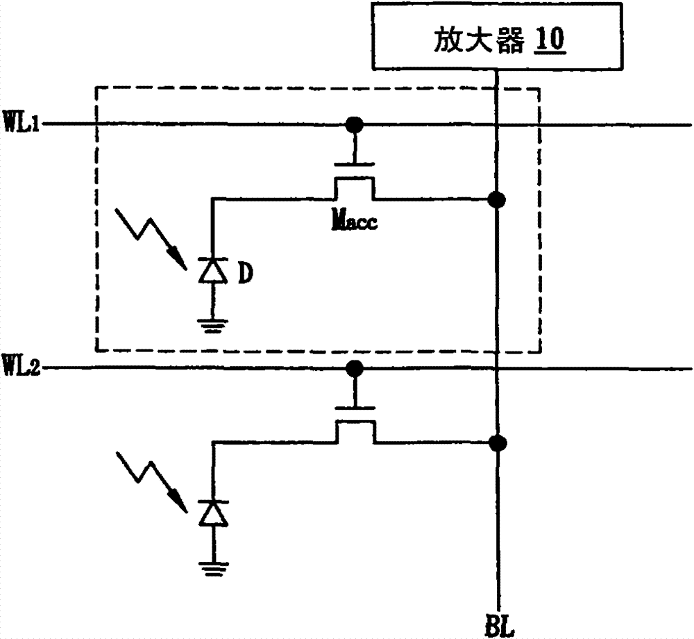
[0045] Figure 2AA four-transistor (4T) pixel circuit of a complementary metal-oxide-semiconductor (CMOS) image sensor according to an embodiment of the present invention is shown, which is shared (4S) by four pixels. In this embodiment, the overall area of ​​the pixel array of the CMOS image sensor can be reduced, or more space can be reserved for the photodiode. In this embodiment (and other embodiments in this specification), the pixel circuit is shared by four pixels, but not limited to four; moreover, the pixel circuit of the present invention is not limited to contain four transistors (4T ), for example, may also be 5T or more transistors. In the illustrated 4T 4S pixel circuit, four photodetectors (such as pinned photodiodes) D corresponding to four pixels 1 -D 4 respectively connected to the pass transistor M tx1 -M tx4 . In this embodiment, the transfer transistor M tx1 -M tx4 It is an n-type metal oxide semiconductor (NMOS) transistor. Photodiode D 1 -D 4 ...


PUM


Abstract

The invention provides a pixel circuit of a CMOS (complementary metal oxide semiconductor) image sensor, which is characterized by using at least two transferring transistors for respectively transferring the accumulated optical signals of corresponding photodetectors to a first node, using a resetting transistor for resetting the voltage of the first node as the preset resetting voltage of a second node, and using a source follower for buffering the integrated optical signals. In the embodiment of the invention, a capacitor is connected between the first node and the second node, so as to reduce the impact of the effective capacitance comprising the capacitance in the floating diffusion areas and the stray capacitance in the photodetectors and transferring transistors.

Description

technical field [0001] The present invention relates to a complementary metal oxide semiconductor (CMOS) image sensor, in particular to a pixel readout circuit (pixel readout circuit) of a CMOS image sensor with a smaller area, and a pixel readout circuit with a feedback (or switching) capacitance out of the circuit. Background technique [0002] A CMOS image sensor is an electronic device that captures images, such as those used in cameras, and converts light intensity into electric charge, which is then converted into voltage and read out. Figure 1A A passive pixel sensor (PPS), which is a type of conventional CMOS image sensor, is shown. For ease of illustration, only two pixels in the pixel array are shown in the figure. Each pixel contains a photodiode (photodiode) D and access transistor (or switch) M acc . word line (such as WL 1 ) are connected to pixels in the same row, while bit lines (such as BL) are connected to pixels in the same column. At the end of each...

Claims


Application Information

Patent Timeline
Patent Type & Authority Patents(China)
IPC IPC(8): H04N5/374H04N5/378
CPCH04N25/59
Inventor 印秉宏米特拉·艾米特林积劭
Owner HIMAX IMAGING LIMITED
Why Eureka
Try Eureka