Optical waveguide, method for manufacturing the optical waveguide, and optical device provided with the optical waveguide

A technology of optical waveguides and optical devices, applied in the directions of light guides, optical components, instruments, etc., can solve the problems of enlarged space, limited dispersion compensation characteristics, difficult miniaturization, etc., and achieve the degradation of S/N ratio reduction and dispersion compensation. Wide range of features and reduced setting space

Inactive Publication Date: 2010-12-01
FUJIKURA LTD
View PDF5 Cites 0 Cited by
  • Summary
  • Abstract
  • Description
  • Claims
  • Application Information

AI Technical Summary

Problems solved by technology

[0026] 1: Dispersion compensation using DCF requires a larger space due to the use of longer optical fibers, making it difficult to miniaturize
Furthermore, there is a limit to the dispersion compensation characteristics that can be achieved
[0027] 2: When using FBG, there is a limit to the change of the refractive index of the fiber
[0029] 4: When using AWG, the structure is complicated, the manufacturing is difficult, and the cost becomes higher
In addition, a large space is required, and it is difficult to miniaturize the device
[0030] 5: The structure of the VIPA type dispersion compensator is complicated, the manufacture is difficult, and the cost becomes high
[0031] 6: In the gain equalizer using liquid crystal, the structure of the device is complicated
Therefore, manufacturing is difficult and the cost becomes high

Method used


Image

  • Optical waveguide, method for manufacturing the optical waveguide, and optical device provided with the optical waveguide
  • Optical waveguide, method for manufacturing the optical waveguide, and optical device provided with the optical waveguide
  • Optical waveguide, method for manufacturing the optical waveguide, and optical device provided with the optical waveguide

Examples


Embodiment 1

[0190]Designed in the wavelength region [1545nm~1555nm], the dispersion amount D=-10ps / nm, the ratio of dispersion slope to dispersion RDS=0.0034nm -1 A dispersion compensation device for compensation of wavelength dispersion. The dispersion compensating device is mainly used for compensating the dispersion not fully compensated by the DCF because the amount of dispersion to be compensated is relatively small.

[0191] Figure 5 is a graph showing the potential distribution of the NPWG of the dispersion compensation device fabricated in this example. The horizontal axis in the figure represents the position normalized with the center wavelength of 1550 nm. Using this potential, we get Figure 6 The group delay characteristics shown and the Figure 7 The reflectance characteristics shown. The spectral data used in the design (designed) and the obtained spectral data (realized) are shown in two figures.

[0192] The NPWG of this embodiment adopts h 3 =6 μm and a relative ...

Embodiment 2

[0197] Designed in the wavelength region [1545nm~1555nm], the dispersion amount D=-50ps / nm, the ratio of dispersion slope to dispersion RDS=0.0034nm -1 A dispersion compensation device for compensation of wavelength dispersion. The dispersion compensating device is also similar to the first embodiment, and is mainly used for compensating the dispersion not fully compensated by the DCF.

[0198] Figure 13 is a graph showing the potential distribution of the NPWG of the dispersion compensation device fabricated in this example. The horizontal axis in the figure represents the position normalized with the center wavelength of 1550 nm. Using this potential, we get Figure 14 The group delay characteristics shown and the Figure 15 The reflectance characteristics shown. The spectral data used in the design (designed) and the obtained spectral data (realized) are shown in two figures.

[0199] The NPWG of this embodiment adopts h 3 =6 μm and a relative refractive index diffe...

Embodiment 3

[0201] Designed in the wavelength region [1545nm~1555nm], the dispersion amount D=-100ps / nm, the ratio of dispersion slope to dispersion RDS=0.0034nm -1 A dispersion compensation device for compensation of wavelength dispersion. The dispersion compensation device is also similar to the above-mentioned embodiments, and is mainly used for compensating the dispersion not fully compensated by the DCF. In this embodiment, it is possible to compensate the wavelength dispersion of a standard single-mode fiber (S-SMF: Standard Single-Fiber) with a length of about 6 km.

[0202] Figure 18 is a graph showing the potential distribution of the NPWG of the dispersion compensation device fabricated in this example. The horizontal axis in the figure represents the position normalized with the center wavelength of 1550 nm. Using this potential, we get Figure 19 The group delay characteristics shown and the Figure 20 The reflectance characteristics shown. The spectral data used in the...


PUM


Abstract

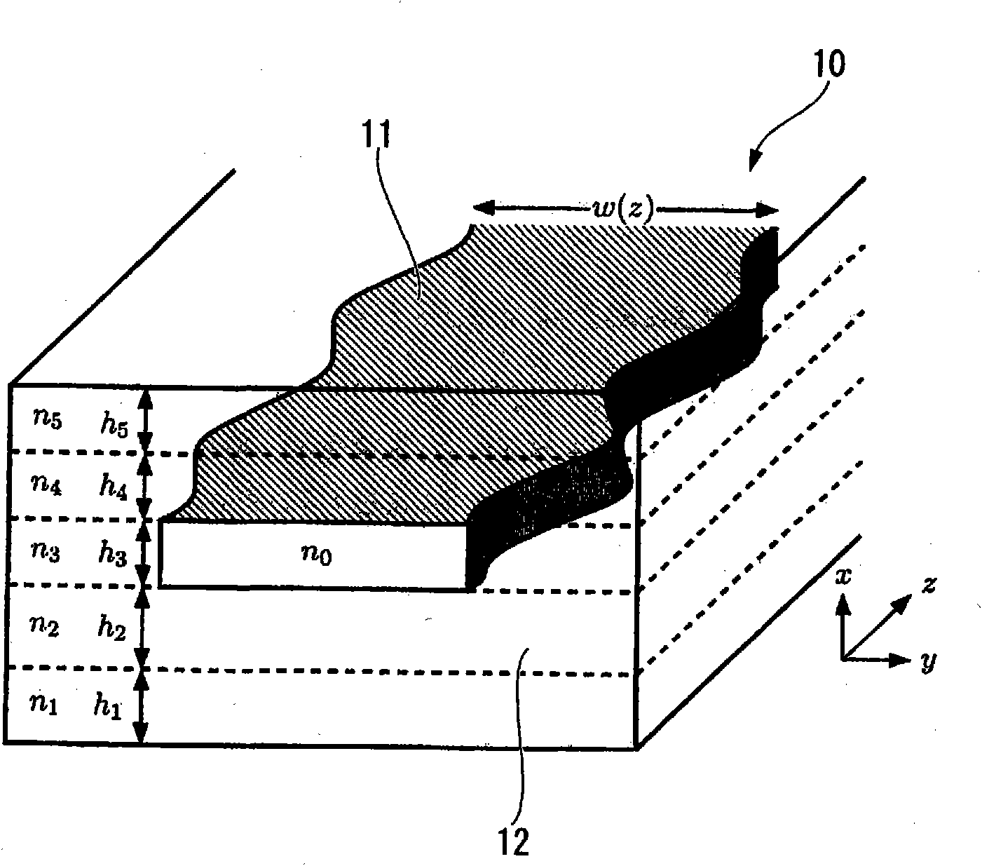
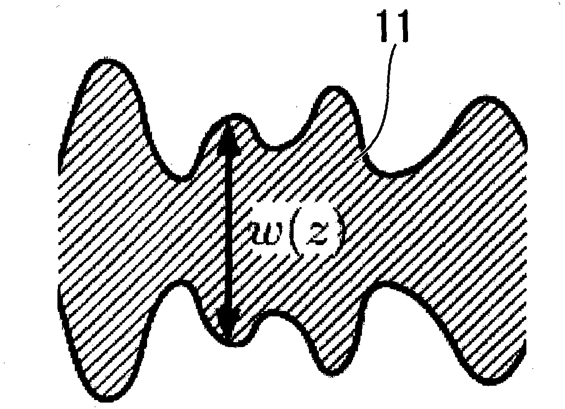
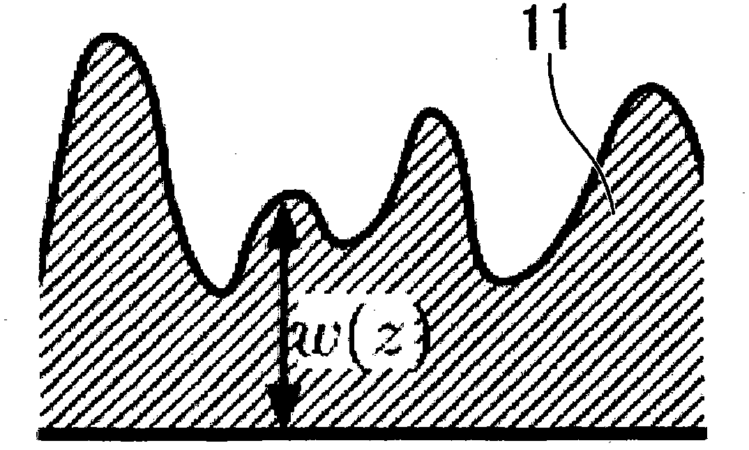
The invention provides an optical waveguide, a method for manufacturing the optical waveguide, and an optical device provided with the optical waveguide. The optical waveguide is provided with a clad and a core embedded in the clad. The equivalent refractive index of the core is nonuniformly varied over the light propagating direction by changing the physical dimensions of the core.

Description

technical field [0001] The present invention relates to a reflective optical waveguide, its manufacturing method and an optical device with the optical waveguide. The optical device can be used in optical fiber communication network, etc. [0002] This application claims priority based on Patent Application No. 2007-331004 for which it applied in Japan on December 21, 2007, and takes in the content into this application. Background technique [0003] In optical communication, wide-band and high-speed transmission of high-density wavelength multiplexing (DWDM: Dense Wavelength-Division Multiplexing) is constantly developing. [0004] In order to perform high-speed transmission, it is desirable for the transmission line to have as small a wavelength dispersion as possible in the transmission band, and to suppress nonlinear effects, it is desirable to use an optical fiber with non-zero wavelength dispersion. However, optical fibers that have already been laid over a wide rang...

Claims


Application Information

Patent Timeline
Patent Type & Authority Applications(China)
IPC IPC(8): G02B6/122
CPCG02B6/124
Inventor 官宁小川宪介
Owner FUJIKURA LTD
Why Eureka
Try Eureka