Semiconductor device

A semiconductor, conductive type technology, applied in the direction of semiconductor devices, electrical components, circuits, etc., can solve the problems of increased loss and increased on-resistance, and achieve the effect of preventing the reduction of withstand voltage

Active Publication Date: 2012-08-08
FUJI ELECTRIC CO LTD
View PDF3 Cites 0 Cited by
  • Summary
  • Abstract
  • Description
  • Claims
  • Application Information

AI Technical Summary

Problems solved by technology

Conversely, in a semiconductor element with a high withstand voltage, the drift layer is thicker, so the on-resistance becomes larger, resulting in an increase in loss

Method used


Image

  • Semiconductor device
  • Semiconductor device
  • Semiconductor device

Examples


Embodiment 2

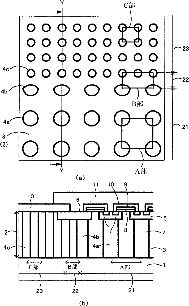
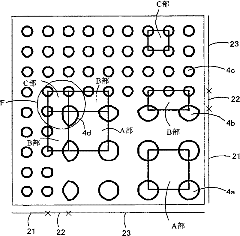
[0076] Figure 4 With figure 1 (a) A plan view of the main part of the semiconductor device corresponding to the second embodiment of the present invention. The difference from Embodiment 1 is that the planar shape of the p isolation region 4e and the n drift region 3a of the active region 21 is stripe. As in Example 1, when the impurity dose of the p isolation region 4e is four times the impurity dose of the n drift region 3a, the area of ​​the p isolation region 4e in the D part of the active region 21 is the area of ​​the D part. 1 / 4 of that, thus, charge balance can be achieved, and a decrease in withstand voltage can be prevented.

[0077] The shape and size of the p-isolation region of the termination region 23 are the same as those of the p-isolation region of Embodiment 1.

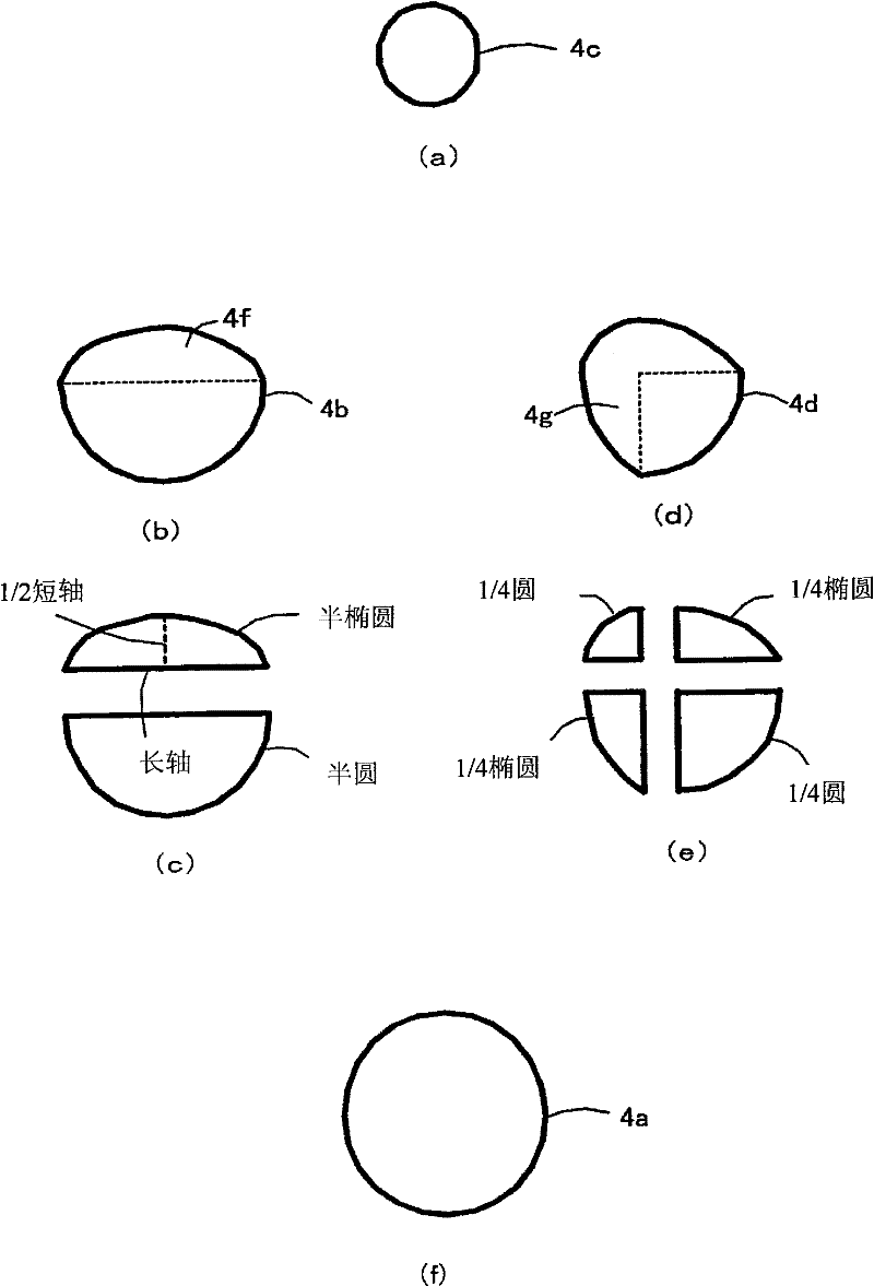
[0078] in addition, Figure 4 The p isolation regions 4f, 4g of the transition region 22 on the side of the active region 21 and the image 3 (b), image 3 Parts 4f and 4g of the p isolation ...


PUM


Abstract

The invention provides a semiconductor device which can realize charge balance in a unit of a transition region under the condition that an active region and a terminal region change internal of units, thereby preventing withstand voltage reduction. The shape of p isolation region of the transition region (22) is changed corresponding to the active region (21) and the terminal region (23). Chargebalance is realized in each p isolation regions (4a), (4b), (4c) and n drift region (3) of the active region (21), the transition region (22) and the terminal region (23), thereby realizing prevention of withstand voltage reduction.

Description

technical field [0001] The present invention relates to a semiconductor device such as a MOSFET (insulated gate field effect transistor) having a super junction (SJ: Super Junction) structure capable of achieving both a high withstand voltage and a large current capacity. Background technique [0002] Generally, semiconductor elements are classified into horizontal elements in which electrodes are formed on one surface of a semiconductor substrate and vertical elements in which electrodes are formed on both surfaces of a semiconductor substrate. In the case of a vertical semiconductor element, the direction in which the drift current flows in the ON state is the same as the direction in which the depletion layer expands due to the reverse bias voltage in the OFF state. In a normal planar n-channel vertical MOSFET, the high-resistance drift layer functions as a region where a drift current flows in the vertical direction in the on state. Therefore, if the current path of the...

Claims


Application Information

Patent Timeline
Patent Type & Authority Patents(China)
IPC IPC(8): H01L29/78H01L29/06
Inventor 北村睦美武井学
Owner FUJI ELECTRIC CO LTD
Why Eureka
Try Eureka