Semiconductor device and power conversion device

a technology of a power conversion device and a semiconductor, which is applied in the direction of semiconductor devices, basic electric elements, electrical appliances, etc., can solve the urgent and important problem of reducing the power loss of the power conversion device, and achieve the effect of preventing a decrease in the voltage resistance, reducing the forward voltage drop and the backward recovery curren

Active Publication Date: 2022-03-22
HITACHI POWER SEMICON DEVICE
View PDF12 Cites 0 Cited by
  • Summary
  • Abstract
  • Description
  • Claims
  • Application Information

AI Technical Summary

Benefits of technology

[0022]The invention provides a semiconductor device for an inexpensive flywheel diode capable of decreasing a forward voltage drop and a backward recovery current and preventing a decrease in a voltage resistance, and a power conversion device using the semiconductor device.

Problems solved by technology

Therefore, how to reduce a power loss of the power conversion device is an urgent and important problem.

Method used


Image

  • Semiconductor device and power conversion device
  • Semiconductor device and power conversion device
  • Semiconductor device and power conversion device

Examples


first embodiment

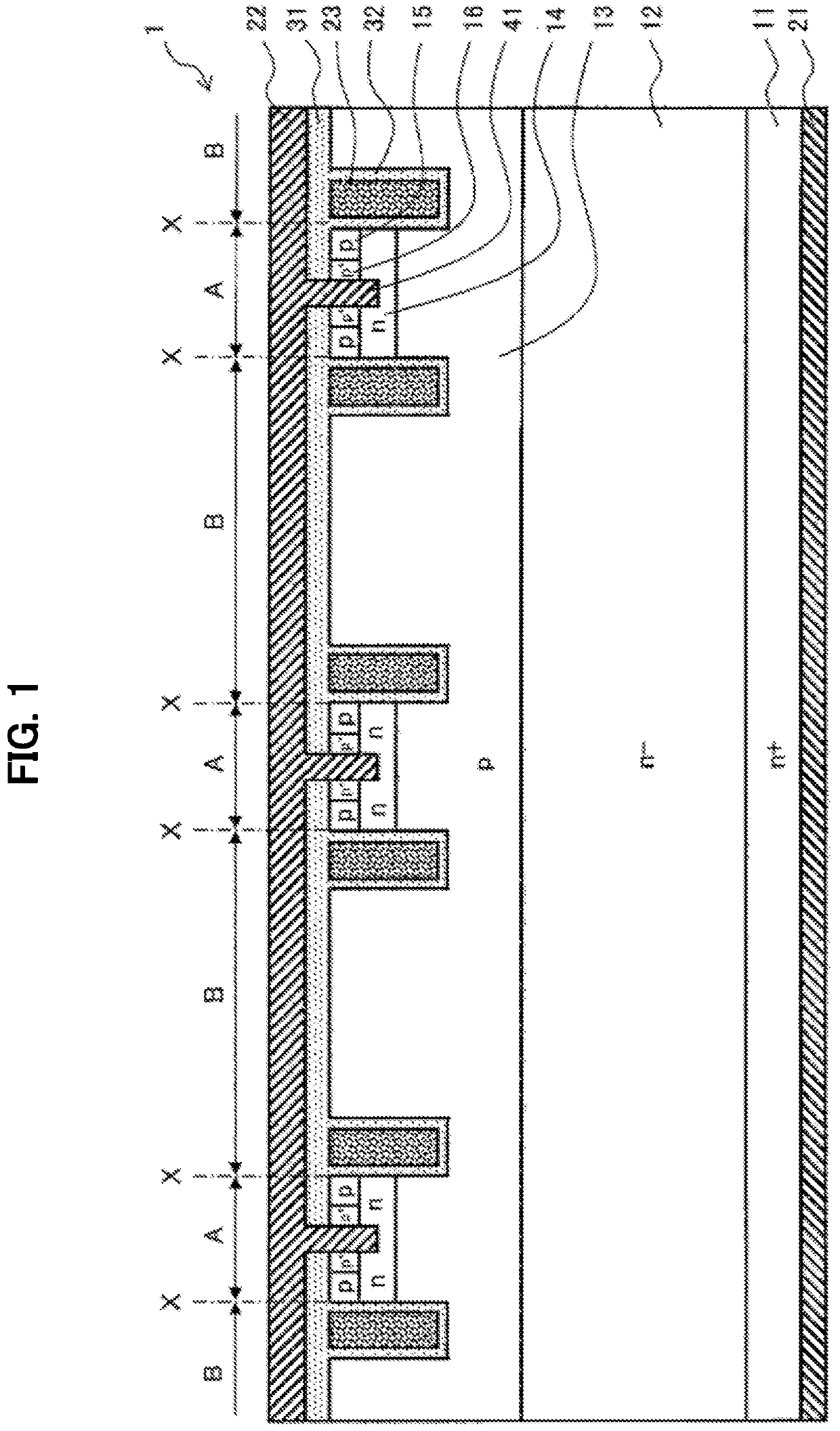
[0047]FIG. 1 is a diagram showing an example of a cross-sectional structure of a semiconductor device 1 according to a first embodiment of the invention. As shown in FIG. 1, a semiconductor substrate of the semiconductor device 1 includes an n+ layer 11, an n− layer 12, a p layer 13, an n layer 14, a p layer 15, and a p+ layer 16. A cathode electrode 21 is in electrical contact with the n+ layer 11 at a low resistance. On the other hand, on a side of an anode electrode 22, the p+ layer is provided in the p layer 15, and at least a part of the p+ layer 16 is in contact with the anode electrode 22 at a low resistance. In addition, a Schottky junction is formed between the anode electrode 22 and the n layer 14.

[0048]A gate electrode 23 having a trench structure is insulated from the semiconductor substrate and the anode electrode 22 via a gate insulating film 32 and an insulating film 31. A side of the semiconductor substrate of the gate insulating film 32 is surrounded by the p layer ...

second embodiment

[0072]FIG. 10 is a diagram showing an example of a cross-sectional structure of the semiconductor device 2 according to a second embodiment of the invention. The semiconductor device 2 according to the second embodiment and the semiconductor device 1 according to the first embodiment are different depending on whether the gate electrode 23 is in contact with one side surface or both side surfaces of the semiconductor substrate. That is, in the semiconductor device 1 shown in FIG. 1, both side surfaces of the gate electrode 23 are in contact with the semiconductor substrate (the p layer 13, the n layer 14, and the p+ layer 16) via the gate insulating film 32. In contrast, in the semiconductor device 1 according to the present embodiment, one side surface of the gate electrode 23 is in contact with the semiconductor substrate (the p layer 13, the n layer 14, and the p+ layer 16) via the gate insulating film 32, and another side surface is in contact with a thick insulating film 31. In...

third embodiment

[0074]FIG. 11 is a diagram showing an example of a cross-sectional structure of a semiconductor device 3 according to a third embodiment of the invention. The semiconductor device 3 according to the third embodiment differs from the semiconductor device 1 according to the first embodiment (see FIG. 1) in that the semiconductor device 3 has a planar structure in which the gate electrode 23 is provided on the surface of the semiconductor substrate. The semiconductor device 3 having the planar structure has an effect that a manufacturing process is easy since it is not necessary to dig a trench in the semiconductor substrate. The other effects are substantially the same as those of the first embodiment.


PUM

PropertyMeasurementUnit
voltageaaaaaaaaaa
gate voltageaaaaaaaaaa

Abstract

The invention provides an inexpensive flywheel diode having a low power loss. A semiconductor substrate side of a gate electrode provided on a surface of an anode electrode side of a semiconductor substrate including silicon is surrounded by a p layer, an n layer, and a p layer via a gate insulating film. The anode electrode is in contact with the p layer with a low resistance, and is also in contact with the n layer or the p layer, and a Schottky diode is formed between the anode electrode and the n layer or the p layer.

Description

TECHNICAL FIELD[0001]The present invention relates to a semiconductor device suitable for controlling switching of a large current and a power conversion device using the semiconductor device.BACKGROUND ART[0002]At present, a power conversion device such as an inverter or a converter is widely used from home appliances such as air conditioners, refrigerators, and electromagnetic cookers, to industrial and automotive equipment such as electric vehicles, uninterruptible power supply, solar power generation, and wind power generation, and high-voltage and high-power equipment such as railway, construction machinery, steel and grid power. Such a power conversion device for energy saving or new energy is a key component in realizing a low-carbon society. Therefore, how to reduce a power loss of the power conversion device is an urgent and important problem.[0003]Therefore, in order to reduce power loss of the power conversion device, reduction of the power loss in each circuit component ...

Claims


Application Information

Patent Timeline
Patent Type & Authority Patents(United States)
IPC IPC(8): H01L29/47H01L29/78H01L29/868
CPCH01L29/47H01L29/78H01L29/868H01L29/872H01L29/7397H01L29/7396H01L29/66348H01L29/7391H01L29/4236H01L29/407H01L29/0834
Inventor MORI, MUTSUHIROMIYOSHI, TOMOYUKIFURUKAWA, TOMOYASUSHIRAISHI, MASAKI
Owner HITACHI POWER SEMICON DEVICE
Why Eureka
Try Eureka