
Dynamic statistic sampling control method and device for on-line defect scanning

A defect scanning and dynamic statistics technology, applied in electrical program control, semiconductor/solid-state device manufacturing, program control in sequential/logic controllers, etc., can solve the problem of increased cost, particles attached to the wafer, unable to alert maintenance personnel, etc. problems, to avoid lengthening, avoid cost increases, and enhance defect monitoring

Inactive Publication Date: 2012-11-28
SEMICON MFG INT (SHANGHAI) CORP +1
View PDF5 Cites 0 Cited by
  • Summary
  • Abstract
  • Description
  • Claims
  • Application Information

AI Technical Summary

Problems solved by technology

The disadvantage of this sampling method is that when the batches of wafers processed in the process step do not meet the set sampling conditions for a period of time, no wafers are scanned for online defects during this period
That is, this sampling method may not be able to monitor the process step in real time for a long period of time
There is no way to alert maintenance personnel if a process step fails during this time, allowing particulates or other defects to form on the wafer
[0004] On the other hand, if most of the wafers processed in the process steps meet the set sampling conditions within a period of time, a large number of wafers will enter the online defect scanning during this period, which will lengthen the production process and increase the cost. cause unnecessary waste

Method used


Image

  • Dynamic statistic sampling control method and device for on-line defect scanning
  • Dynamic statistic sampling control method and device for on-line defect scanning
  • Dynamic statistic sampling control method and device for on-line defect scanning

Examples


Embodiment Construction

[0020] The present invention will be described in detail below in conjunction with the accompanying drawings and specific embodiments.

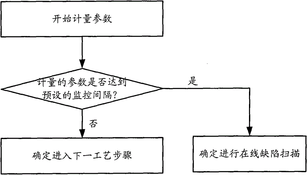
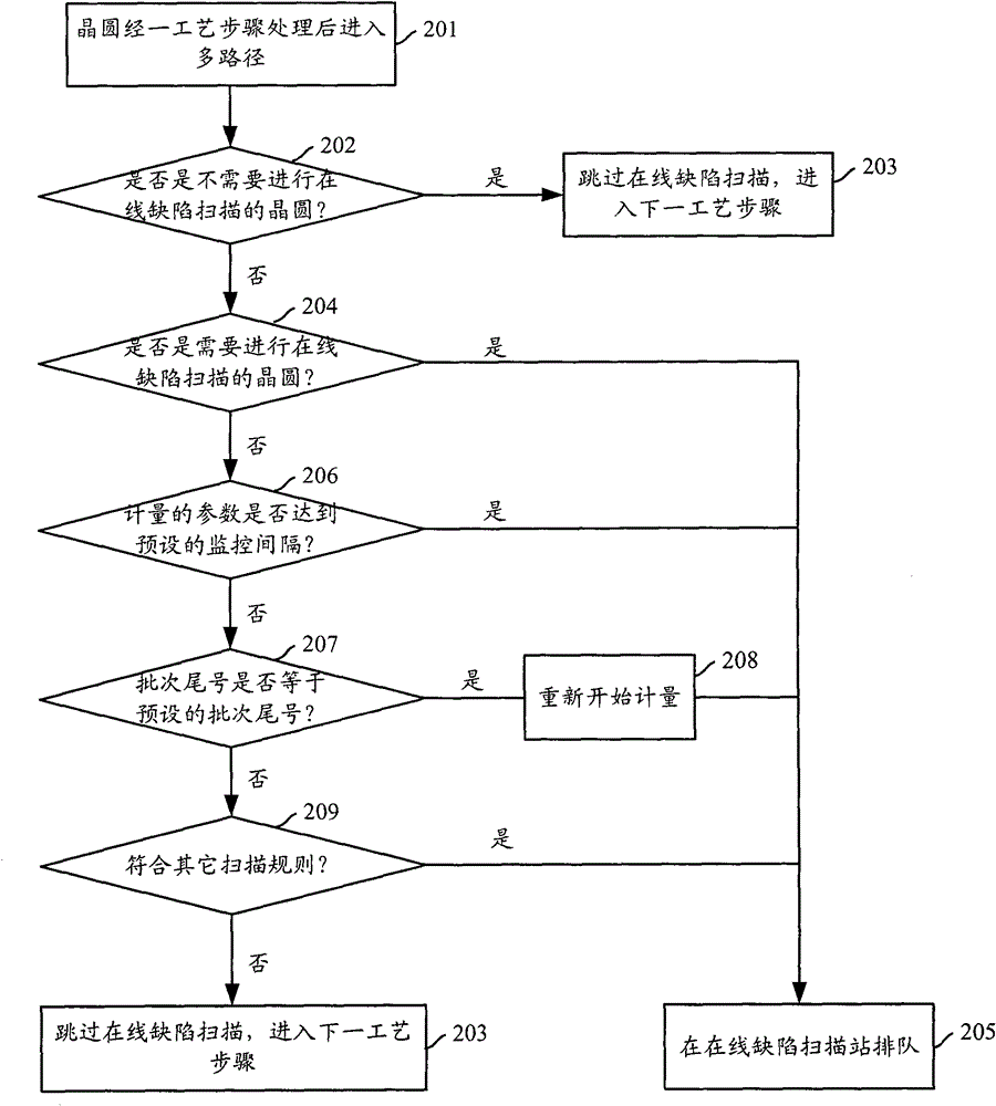
[0021] figure 1 It is a flow chart of the dynamic statistical sampling control method for online defect scanning of the present invention. see figure 1 The dynamic statistical sampling control method for online defect scanning provided by the present invention determines whether online defect scanning needs to be performed on wafers processed in process steps by judging whether the metering parameters have reached a preset monitoring interval. Specifically, if the metered parameters reach the preset monitoring interval, it is determined to perform online defect scanning on the wafer processed by the process step, otherwise it is determined to perform the next process step on the wafer processed by the process step, so that The problem of being unable to monitor wafer defects for a period of time and monitoring a large number of wafers for a...


PUM


Abstract

The invention discloses a dynamic statistic sampling control method for on-line defect scanning, which comprises the following steps of: beginning to meter parameters; judging whether the metered parameters reach the preset monitoring intervals or not; and determining to carry out on-line defect scanning on wafers processed by the process steps if the metered parameters reach the preset monitoring intervals, or determining to carry out next process step treatment on the wafer processed by the process steps. The invention also discloses a dynamic statistic sampling control device for the on-line defect scanning. The method and the device can be used for avoiding the problem of unbalanced sampling monitoring wafer number in a period of time, enhancing the defect monitoring on the productionline and avoiding the production process prolonging and the cost increase.

Description

technical field [0001] The invention relates to the field of semiconductor manufacturing, in particular to a dynamic statistical sampling control method and device for online defect scanning. Background technique [0002] Usually in the process flow of a semiconductor manufacturing plant, after some key process steps, the wafer will be scanned for defects online. The purpose of setting the online defect scan is to monitor whether there are particles attached to the wafer or whether other defects are formed after the current critical process. Because in these critical process steps, if there are particles attached or other defects formed on the wafer, it may affect the performance of the subsequently formed devices. Therefore, it is very important to monitor the wafer for particle attachment or defect formation. [0003] In the prior art, when sampling wafers, by setting the batch tail number, the wafers meeting the set sampling conditions will be scanned for defects online...

Claims


Application Information

Patent Timeline
Patent Type & Authority Patents(China)
IPC IPC(8): G05B19/04H01L21/00
Inventor 黄辉
Owner SEMICON MFG INT (SHANGHAI) CORP
Learn More