

Fast recovery diode
A fast recovery, diode technology, applied in the direction of semiconductor devices, electrical components, circuits, etc., can solve the problems of strong changes in leakage current and high leakage current of diodes
- Summary
- Abstract
- Description
- Claims
- Application Information
AI Technical Summary
Problems solved by technology
Method used
Image

Examples
Embodiment Construction
[0026] Further description will be made using the first conductivity type as the n-type and the second conductivity type as the p-type, but alternatively the conductivity type can also be reversed.
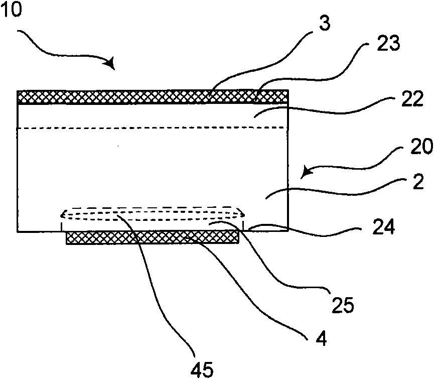
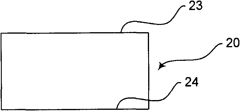
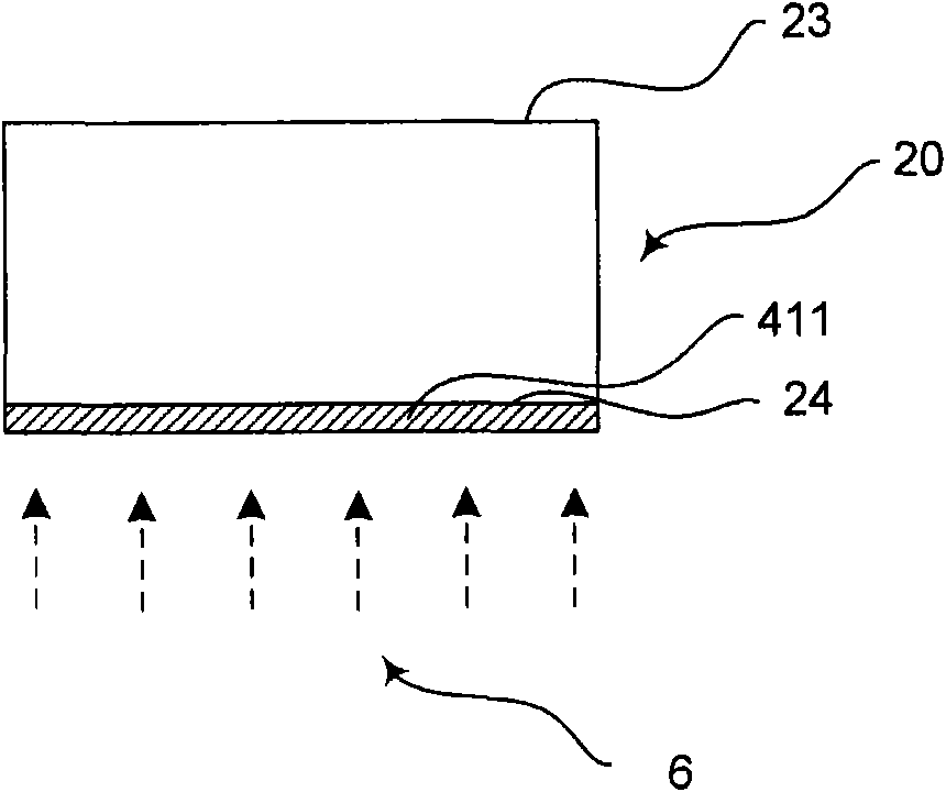
[0027] Picture 12 An inventive fast recovery diode 1 is shown that includes a wafer 20. The portion of the wafer with unmodified doping during the manufacturing process forms a base layer 2 of the first conductivity type (ie, n-type), which has a cathode side 23 and the anode side 24 on the opposite side of the cathode side 23. On the cathode side 23, an n-doped cathode buffer layer 22 may be provided. In the case where the diode 1 has such a cathode buffer layer 22, this layer has a higher doping than the (n-)doped base layer 2. The metal layer as the cathode electrode 3 is provided on top of the cathode buffer layer 22 on the side opposite to the base layer 2.
[0028] The metal layer as the anode electrode 4 is provided on the anode side of the wafer 20. The p-doped anode contac...
PUM
 Abstract
Description
Claims
Application Information