

Wafer exposure method
An exposure method and wafer technology, which are applied in microlithography exposure equipment, photolithography process exposure devices, etc., can solve problems such as poor exposure, and achieve the effect of avoiding poor exposure.
- Summary
- Abstract
- Description
- Claims
- Application Information
AI Technical Summary
Problems solved by technology
Method used
Image

Examples
Embodiment Construction
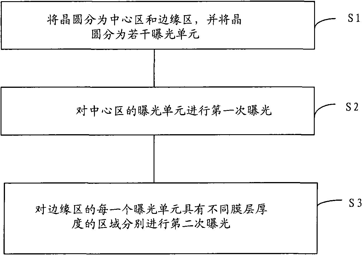
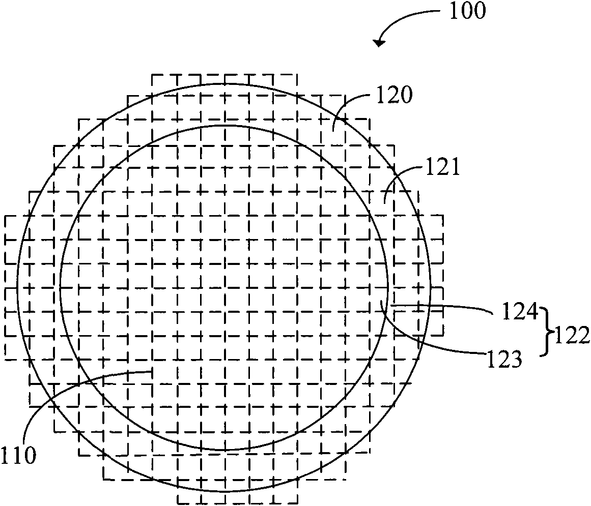
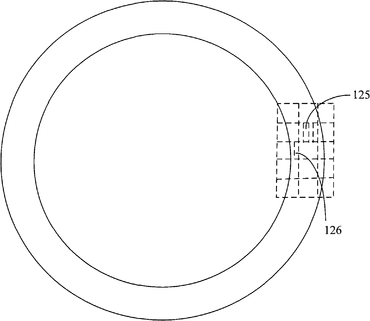
[0025] In the semiconductor exposure process, the exposure process is usually performed by forming a photoresist layer on a wafer with several layers of film layers. In fact, each film layer is not evenly distributed on the entire wafer surface. Generally, near the center of the wafer The film layers in the area of the wafer are evenly distributed and the surface is flat. Therefore, when exposing the exposure unit in the central area of the wafer, there will be no problem of poor exposure in some areas due to poor focus; however, the film layers in the edge area of the wafer are not exposed. Evenly distributed, the surface is not flat, so when exposing the exposure units in the edge area of the wafer, some exposure units will deviate from the focal plane and cause poor exposure (such as underexposure), especially in semiconductor manufacturing with feature sizes smaller than 0.18 μm , due to the narrowing of the process window due to the narrowing of the line width, t...
PUM
| Property | Measurement | Unit |
|---|---|---|
| thickness | aaaaa | aaaaa |
Abstract
Description
Claims
Application Information