Display repairing method and display structure after being repaired

A display and post-repair technology, which can be used in instruments, nonlinear optics, optics, etc., and can solve problems such as ink falling off and unsatisfactory effects

Inactive Publication Date: 2011-07-06
AU OPTRONICS CORP
View PDF6 Cites 20 Cited by
  • Summary
  • Abstract
  • Description
  • Claims
  • Application Information

AI Technical Summary

Problems solved by technology

However, since the ink is very easy to peel off from the surface of the polarizer, the effect of this kind of repair is not ideal

Method used


Image

  • Display repairing method and display structure after being repaired
  • Display repairing method and display structure after being repaired
  • Display repairing method and display structure after being repaired

Examples


Embodiment Construction

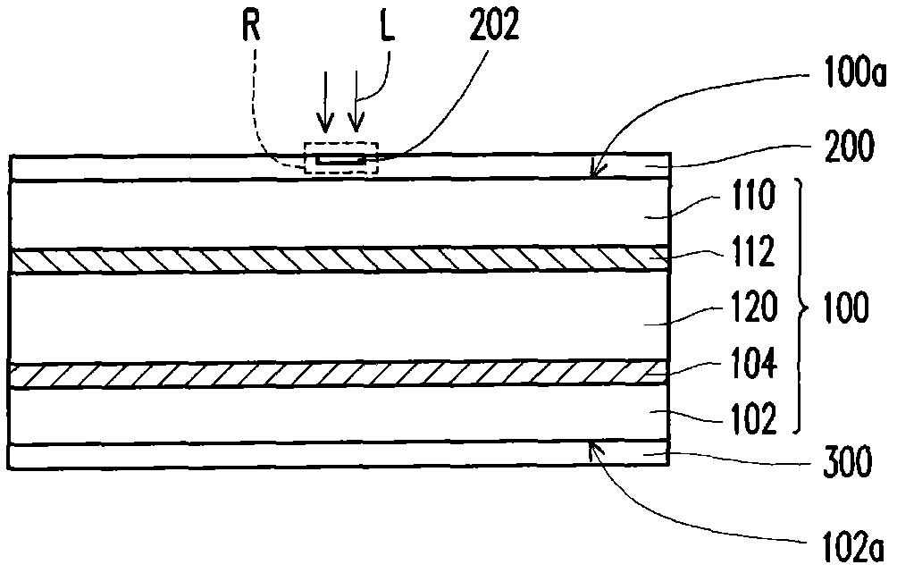
[0015] figure 1 It is a schematic cross-sectional view of a display repair method according to an embodiment of the present invention. Please refer to figure 1 , the repairing method of this embodiment first provides a display, and the display includes a display panel 100 and at least one optical film 200 , 300 .

[0016] The display panel 100 includes a first substrate 102 , a pixel array layer 104 , a second substrate 110 , an electrode layer / color filter layer 112 and a display medium 120 .

[0017] The first substrate 102 and the second substrate 110 are arranged opposite to each other, and the materials of the first substrate 102 and the second substrate 110 can be glass, quartz, organic polymer, or opaque / reflective materials (for example: conductive materials, metal, silicon wafer, ceramics, or other applicable materials), or other applicable materials.

[0018] The pixel array layer 104 is disposed on the first substrate 102 . The pixel array layer 104 includes a p...


PUM

PropertyMeasurementUnit
wavelengthaaaaaaaaaa
thicknessaaaaaaaaaa
sizeaaaaaaaaaa

Abstract

The invention discloses a display repairing method and a display structure after being repaired.According to the method, a display comprising a display panel and at least one optical film is provided.The optical film arranged on at least one outer surface of the display panel comprises an upper surface, a lower surface and an intermediate layer arranged between the upper surface and the lower surface.The optical film equipped with a defect is subject to a laser repairing program, so that the part of the optical film corresponding to the defect is carbonized to be a black point.According to the laser repairing program, black points are formed on the upper surface of the optical film.

Description

technical field [0001] The invention relates to a display repair method and its repaired structure. Background technique [0002] A general liquid crystal panel is composed of an active element array substrate, a color filter substrate, and a liquid crystal layer arranged between the aforementioned two substrates. In addition, the aforementioned two substrates are usually adhered with a frame glue, and the liquid crystal is sealed therebetween. In addition, a polarizer is usually attached to the outer surface of the liquid crystal panel. Through the polarization direction of the polarizer and the twisting direction of the liquid crystal molecules, the bright state or dark state of each pixel unit of the display panel can be controlled. Generally, if there is a defect in the polarizer, a bright spot defect will be generated at a position corresponding to the defect during the operation of the display panel. This is mainly because the above-mentioned defects will cause light...

Claims


Application Information

Patent Timeline
Patent Type & Authority Applications(China)
IPC IPC(8): G02F1/13G02F1/1335
Inventor 梁嘉杉张一凡洪彬哲
Owner AU OPTRONICS CORP
Why Eureka
Try Eureka