Cell switching method and cell switching device
A technology of cell switching and cell, which is applied in the field of data communication, and can solve problems such as increased scheduling complexity, unrealizable number of cross-point buffers, and conflicts
- Summary
- Abstract
- Description
- Claims
- Application Information
AI Technical Summary
Problems solved by technology
Method used
Image

Examples
Embodiment 1
[0125] Only one RAM group is provided in the cell switching device.
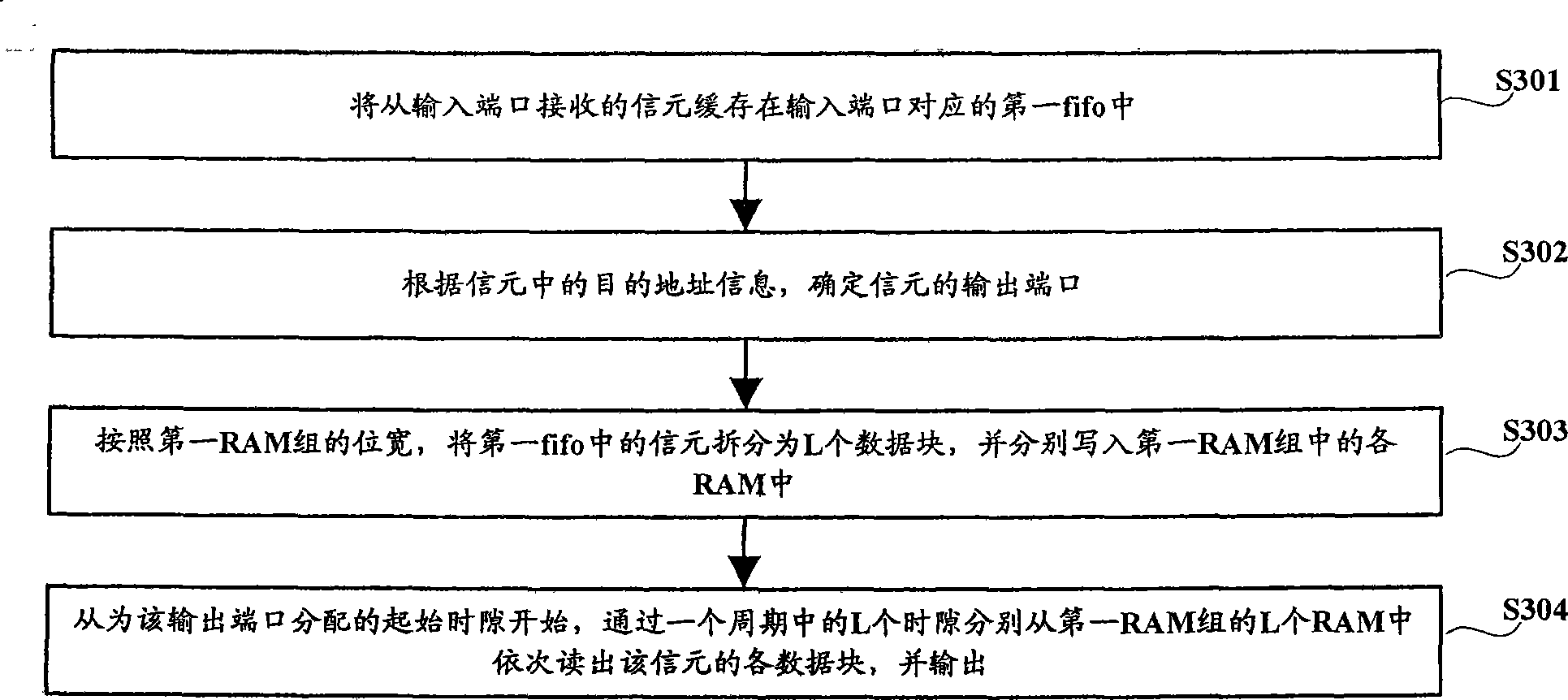
[0126] Such as image 3 As shown, the cell switching method provided by the embodiment of the present invention includes:
[0127] Step S301, buffering the cell received from the input port in the first fifo corresponding to the input port;
[0128] Step S302. Determine the output port of the cell according to the destination address information or destination port information in the cell;
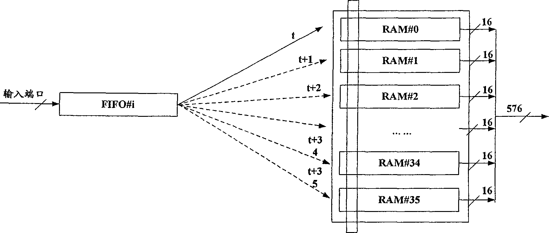
[0129] Step S303, according to the bit width of the first RAM group, the cell in the first fifo is split into L data blocks, and respectively written in each RAM in the first RAM group, the first RAM group includes at least L RAM, the bit width of L=cell length / first RAM;
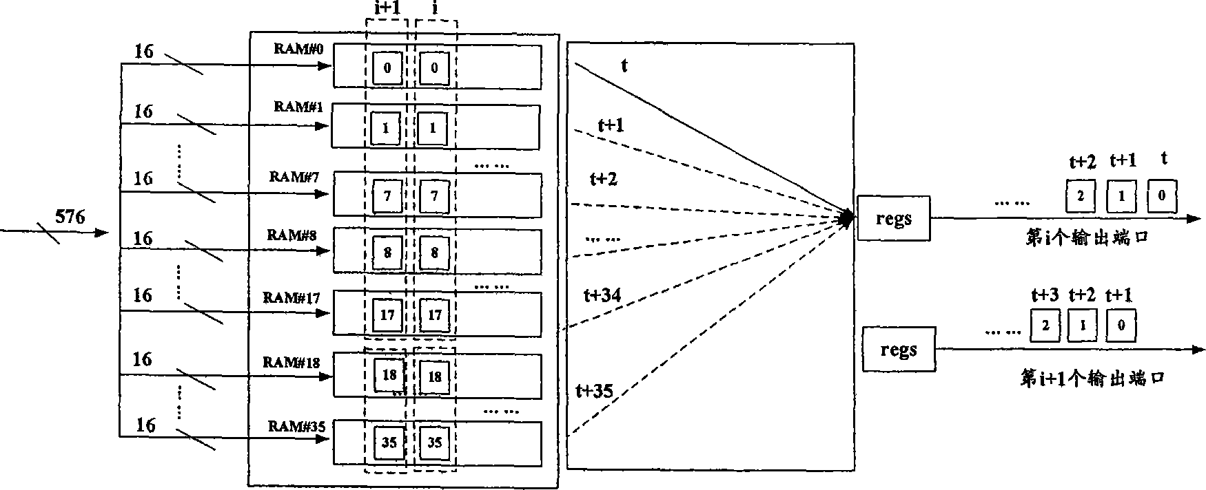
[0130] Step S304, starting from the initial time slot allocated for the output port, through the L time slots in one cycle, read each data block of the cell sequentially from the L RAMs of the first RAM group respectively, and pass the The output ...
Embodiment 2
[0153] Multiple buffers are set in the cell switching device, which is more suitable for the situation where there are many input and output ports.
[0154] At this time, if Figure 5 As shown, the method for cell exchange includes:
[0155] Step S501, buffering the cell received from the input port in the first fifo corresponding to the input port;
[0156] Step S502, according to the bit width of the first RAM group, split the cell in the first fifo into L data blocks, start from the initial time slot allocated for the input port in advance, and pass through L time slots in one cycle Writing L data blocks in turn into the first RAM group corresponding to the group to which the input port belongs, and writing a data block into the corresponding RAM in the first RAM group for each time slot;
[0157] The starting time slots assigned to different input ports are different. In order to ensure that each data block of a cell can be written into the same address of each RAM in th...
PUM
 Abstract
Description
Claims
Application Information