Processor power state transistions using separate logic control

a technology of logic control and power state, applied in the field of computer systems, can solve the problems of not having the ability, unable to support a processor using intel® speedstepTM or similar power conserving technology, and limited processor response to inpu

Inactive Publication Date: 2006-01-17
DELL PROD LP
View PDF12 Cites 59 Cited by
  • Summary
  • Abstract
  • Description
  • Claims
  • Application Information

AI Technical Summary

Benefits of technology

[0029]Problems identified above are addressed by the present disclosure of transitioning power states of processors using separate logic control. This disclosure relates to providing logic that will enable a chipset to transition a power conserving processor into “deep sleep” or C3 state, and also to transition the processor to “operating” or C0 state. This disclosure allows previously non-compatible chipsets to work with power conserving processors, processors frequently used in a mobile PC system.

Problems solved by technology

Many chipsets, namely desktop PC chipsets, do not have the ability to support such a power state transition and therefore cannot support a processor using Intel® Speedstep™ or similar power conserving technology.
While in this state the processor is limited in its ability to respond to input.
Monitoring the Stop Grant Acknowledge bus cycle, however, involves additional expense to add the needed logic.
Power state transition problems arise when either or both the north-bridge controller land the south-bridge controller require special handshaking or messages passed between them during power state transitions that are incompatible.
Because the handshaking / message passing is not compatible, transitions result in a lock up condition such as a controller waiting on a response that never occurs or getting an unexpected / wrong response.
A problem arises as well when a controller, namely a south-bridge controller, has a power management controller that contains logic to detect the Stop Grant Acknowledge bus cycle.
After the controller core logic is configured it is possible that one or both of the controllers may respond poorly to an unexpected Stop Grant Acknowledge bus cycle.
Another problem arises when neither the south-bridge controller nor the north-bridge controller supports power state transitions.
Chipsets and chipset controllers that are not designed to work with power saving processors such as an Intel® Speedstep™ processor are unable to pass power state transition signals through because the controllers lack the necessary control and logic.

Method used


Image

  • Processor power state transistions using separate logic control
  • Processor power state transistions using separate logic control
  • Processor power state transistions using separate logic control

Examples


Embodiment Construction

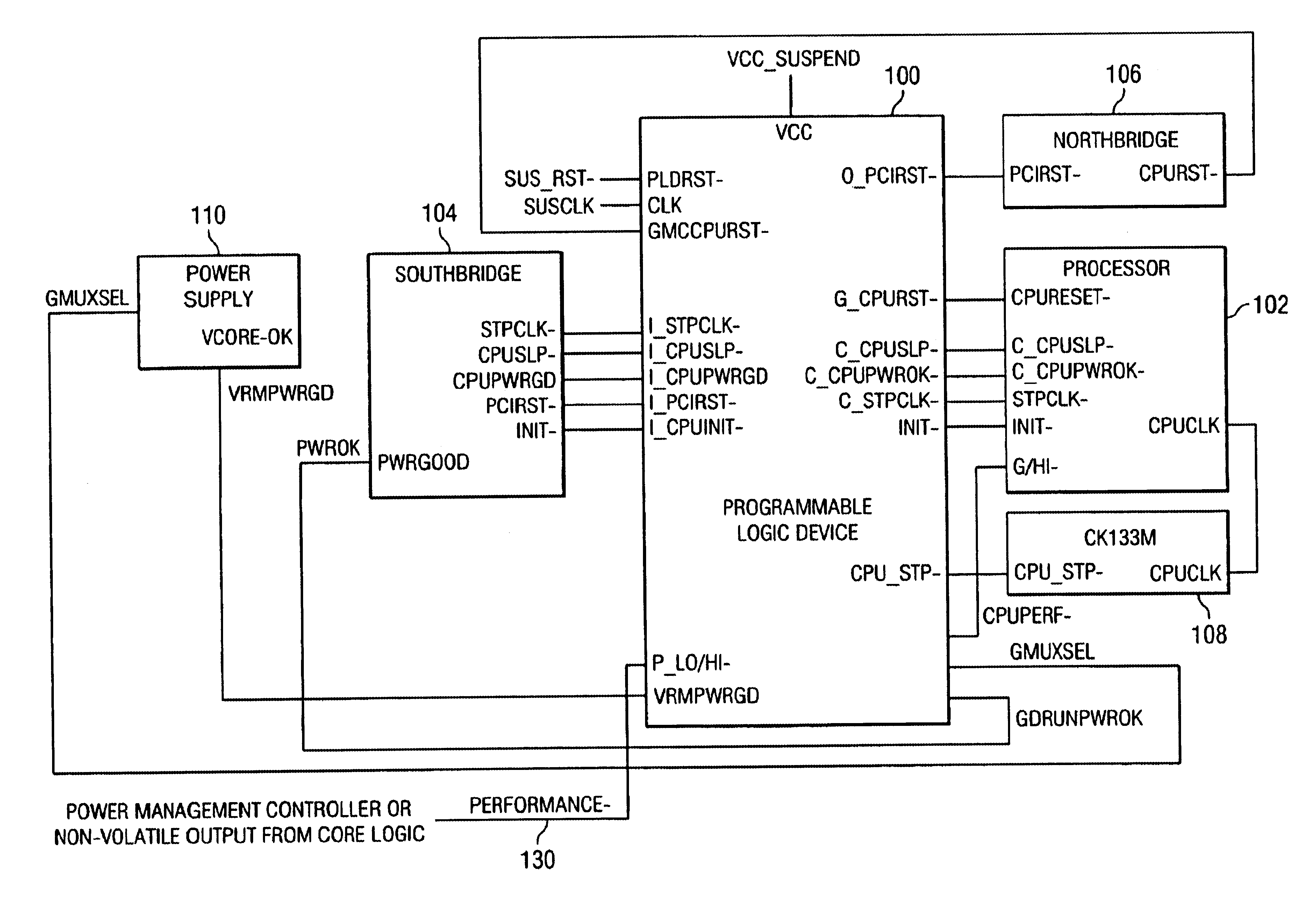
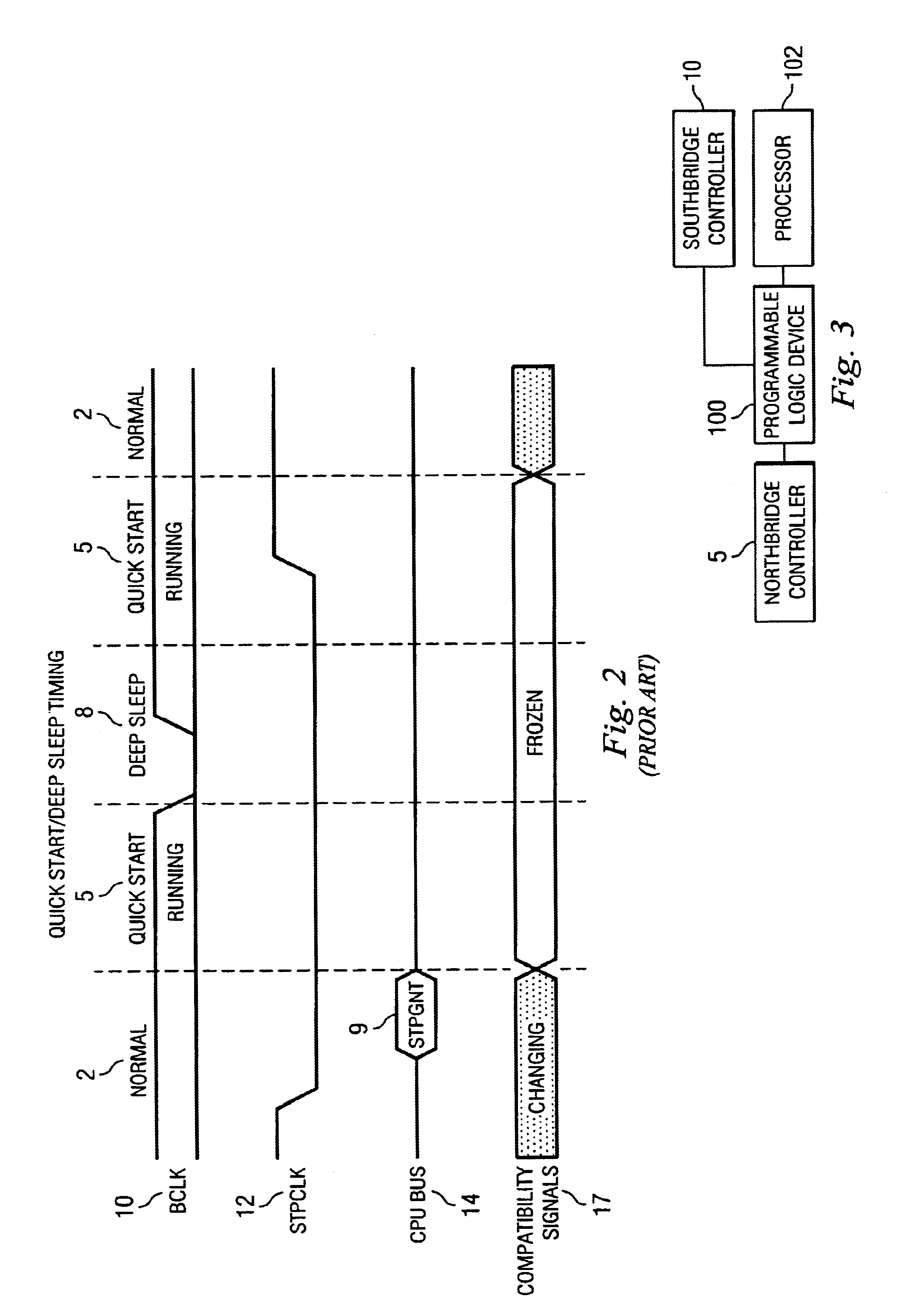
[0047]Now referring to FIG. 3, illustrated is a top level diagram of the PC system showing the interface between chipset controllers, north-bridge controller 5 and south-bridge controller 10 to PLD 100 and processor 102. Select power control signals from north-bridge controller 5 and south-bridge controller 10 are passed to the processor 102 by way of PLD 100. The signals that are passed through PLD 100 are involved in placing the processor into a deep sleep or C3 state and bringing the processor back into operating or C0 state.

[0048]The following table defines the signals used by embodiments of the computer system in performing the processor power state transitions.

[0049]

SignalDefinitionC_CPUPWROKPower OK indication to the processor from the PLDC_CPURST-Processor reset signal from the PLDC_CPUSLP-CPU Sleep control signal to the processor from thePLDC_STPCLK-Processor stop clock signal from the PLDCLKPLD clock inputCPU_STPInput signal to the clock generator that controls theprocesso...


PUM


Abstract

A computer system having a logic device capable of accepting various chipset controllers and interfacing them with a personal computer processor, the logic device capable of placing the processor into a deep sleep state so that the processor can perform power state transitions. The power state transitions place the processor into a battery optimizing mode or a performance optimizing mode. The logic device allows chipset controllers that may or may not have the capability to perform power state transitions to interface with the processor. The logic device either passes power transition signals through to the processor from the chipset controller or performs the power state transitions. Various chipset and chipset controllers may therefore interface with a processor and are able to switch between battery optimized and performance optimized modes.

Description

BACKGROUND[0001]This disclosure relates to a computer system, and more particularly to a mobile computer system using a power conserving processor interfaced with a logic device that allows chipset controllers to pass control signals placing the processor into a deep sleep state or having the logic device place the processor into a deep sleep state in order for the processor to switch power operating modes.DESCRIPTION OF THE RELATED ART[0002]A personal computer's (PC) central processing unit (CPU) or processor is tied directly to the computer system via the chipset. The chipset is the set of controllers on the “motherboard” of a PC, controlling the busses to and from the processor. Often the terms “motherboard” and “chipset” are used interchangeably. Many technologies meet on the motherboard and are “glued” together via the chipset. Without the chipset, neither random access memory (RAM) nor input output (I / O) busses could function together with the processor.[0003]Processors typica...

Claims


Application Information

Patent Timeline
Patent Type & Authority Patents(United States)
IPC IPC(8): G06F1/32
CPCG06F1/3203Y02B60/1214Y02D10/00
Inventor VERDUN, GARY J.
Owner DELL PROD LP
Why Eureka
Try Eureka