Inverter circuit and voltage space vector pulse width modulation method thereof

A voltage space vector, pulse width modulation technology, applied in irreversible DC power input into AC power output, electrical components, AC power input into DC power output, etc. Unbalance and other problems, to achieve the effect of fewer switching actions, continuous operation, and great flexibility

Inactive Publication Date: 2013-12-25
NORTH CHINA ELECTRIC POWER UNIV (BAODING)
View PDF2 Cites 0 Cited by
  • Summary
  • Abstract
  • Description
  • Claims
  • Application Information

AI Technical Summary

Problems solved by technology

Due to the structural characteristics of the diode-clamped three-level inverter itself, the O state leads to the charging and discharging of the DC side capacitors, resulting in unbalanced capacitor voltages. Therefore, the selection of the basic voltage space vector is subject to the capacitor voltage unbalanced problem. limits
Moreover, the state of the same bridge arm is prohibited from directly switching between the P state and the N state, and the O state must be added as a transition state in the middle, which again limits the selection range of the synthetic vector
Although the diode-clamped three-level inverter has increased the number of levels of the output voltage, the maximum amplitude of the fundamental wave of the output line voltage has not increased, and it is still the DC side voltage

Method used


Image

  • Inverter circuit and voltage space vector pulse width modulation method thereof
  • Inverter circuit and voltage space vector pulse width modulation method thereof
  • Inverter circuit and voltage space vector pulse width modulation method thereof

Examples


Embodiment Construction

[0034] The preferred embodiments will be described in detail below in conjunction with the accompanying drawings. It should be emphasized that the following description is only exemplary and not intended to limit the scope of the invention and its application.

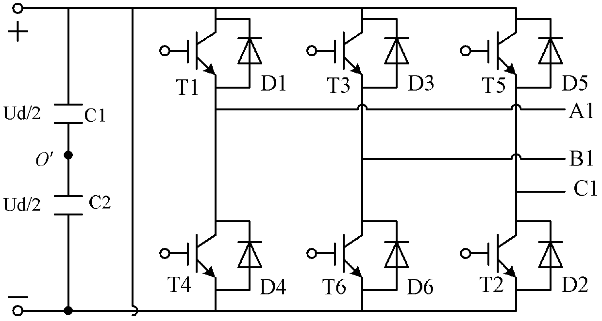
[0035] Figure 4 It is the circuit diagram of the inverter circuit provided by the present invention. Figure 4 Among them, the inverter circuit provided by the present invention includes a DC capacitor C, a first three-phase bridge inverter circuit, a second three-phase bridge inverter circuit and a three-phase isolation transformer T. Wherein, the DC capacitor C is connected across the positive and negative electrodes of the DC power supply on the DC side. The input terminals of the first three-phase bridge inverter circuit and the second three-phase bridge inverter circuit are connected in parallel with the DC capacitor C, and share a DC power supply. The three-phase output terminals of the first three-phase bridge...


PUM


Abstract

The invention discloses an inverter circuit and a voltage space vector pulse width modulation method thereof, which belong to the technical field of circuits. The inverter circuit comprises a direct current capacitor, a first three-phase bridge inverter circuit, a second three-phase bridge inverter circuit and a three-phase isolating transformer. The voltage space vector pulse width modulation method comprises the following steps of: acquiring basic voltage space vectors of the inverter circuit and corresponding switching tube switching state combinations thereof; computing a modulation degree according to an expected voltage space vector; determining the basic voltage space vector for synthesizing the expected voltage space vector according to the modulation degree, finding the corresponding switching tube switching state combinations of the determined basic voltage space vector, and selecting a switching tube switching state combination with the lowest switching frequency from the found switching tube switching state combinations; and regulating a switching tube according to the selected switching tube switching state combination to realize the synthesis of the expected voltage space vector. By the inverter circuit and the method, the problem of voltage unbalance of the direct current capacitor is solved, and the aim of lowest switching frequency in vector switching is fulfilled.

Description

technical field [0001] The invention belongs to the technical field of circuit design, in particular to an inverter circuit and a voltage space vector pulse width modulation method thereof. Background technique [0002] In medium-voltage high-power electric energy conversion applications, multi-level inverter technology has received more and more attention due to its unique advantages. Compared with the traditional two-level inverter circuit, the multi-level inverter has a large number of output voltage levels, less harmonic content, small du / dt caused by switching actions, reduced device withstand voltage requirements, and the same output. Advantages such as low device switching frequency. [0003] Common multi-level structures mainly include diode-clamped multi-level inverters, capacitor-clamped multi-level inverters, and H-bridge cascaded inverters with independent DC power supplies. Taking three-level as an example, diode-clamped three-level inverters and capacitor-cla...

Claims


Application Information

Patent Timeline
Patent Type & Authority Patents(China)
IPC IPC(8): H02M7/49H02M7/5387
Inventor 王文山朱永强赵正奎
Owner NORTH CHINA ELECTRIC POWER UNIV (BAODING)
Why Eureka
Try Eureka